Photonic crystal structure and method of manufacturing the same

Inactive Publication Date: 2008-12-04
CANON KK
View PDF5 Cites 6 Cited by
  • Summary
  • Abstract
  • Description
  • Claims
  • Application Information

AI Technical Summary

Benefits of technology

[0029]According to the present invention, it is possible to provide a photonic crystal structure capable of improving device characteristics. It is also possible to realize a method of manuf

Problems solved by technology

Whereas ideal device characteristics are expected from the three-dimensional photonic crystal having such a microscopic three-dimensional structure as described above, the photonic crystal is generally complex in structure and requires many cumbersome steps for manufacturing.
As a result, requirements for interlayer alignment accuracy and structural processing accuracy become increasingly stringent.
In addition, the interlayer alignment error is desirably less than approximately 25% of the rod period.
This means that the processing error of each rod is less than approximately ±25 nm and each interlayer alignment error is less than approximately ±60 nm.
However, such a conventional laminating method as described in patent document 3 poses the problem, when manufacturing the three-dimensional photonic crystal, that a manufacture method is complex, the number of steps increases in proportion to the number of layers of the photonic crystal and, therefore, the degree of technical difficulty increases, though existing semiconductor technologies can be applied.
Consequently,

Method used


Image

  • Photonic crystal structure and method of manufacturing the same
  • Photonic crystal structure and method of manufacturing the same
  • Photonic crystal structure and method of manufacturing the same

Examples


exemplary embodiment 1

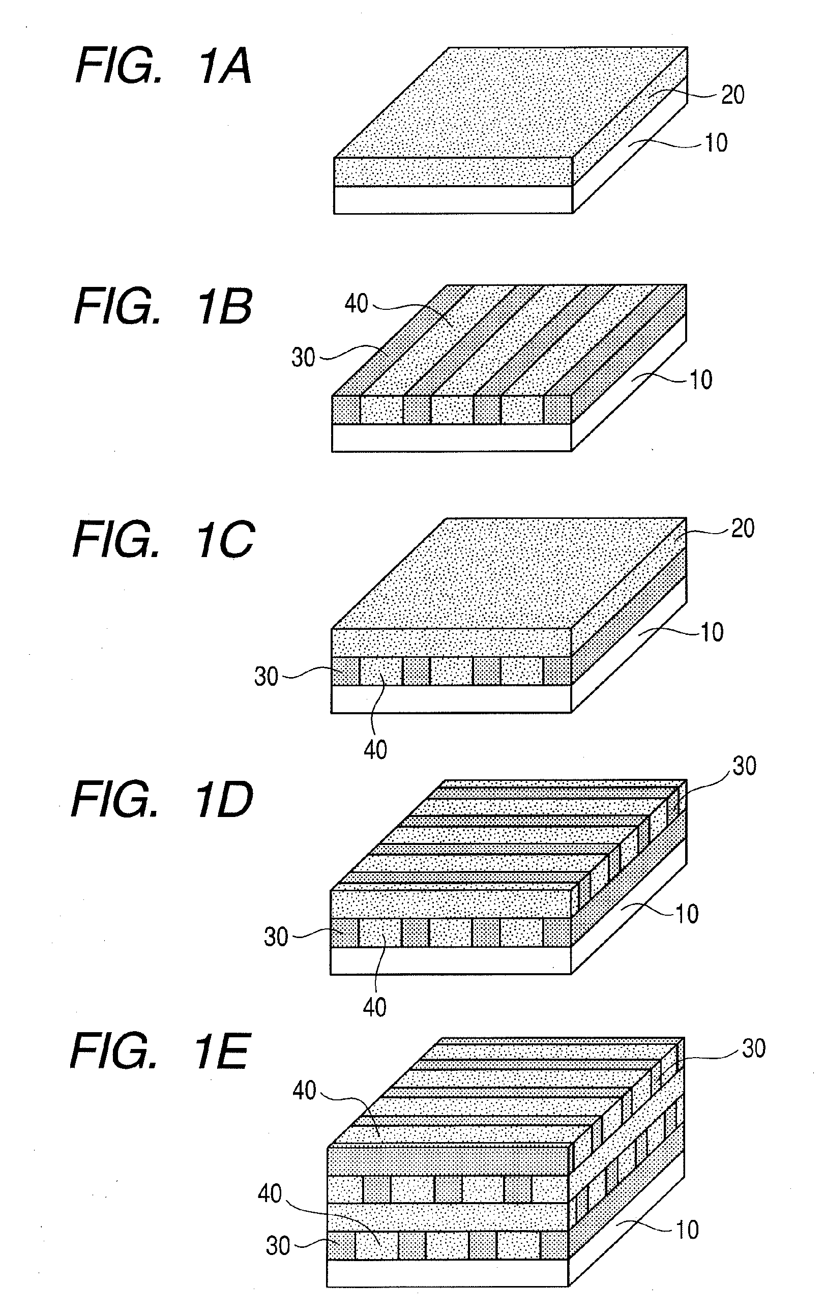
[0052]In exemplary embodiment 1, a description will be made of a method of manufacturing a three-dimensional photonic crystal in which a woodpile structure having a predetermined period is formed by repeating a film-forming step and an ion arrangement step a predetermined number of times. Since the method of manufacturing the three-dimensional photonic crystal in the present exemplary embodiment follows basically the same steps as the method of manufacturing the photonic crystal described in an exemplary embodiment of the present invention, FIGS. 1A to 1E are also used here to describe the present exemplary embodiment.

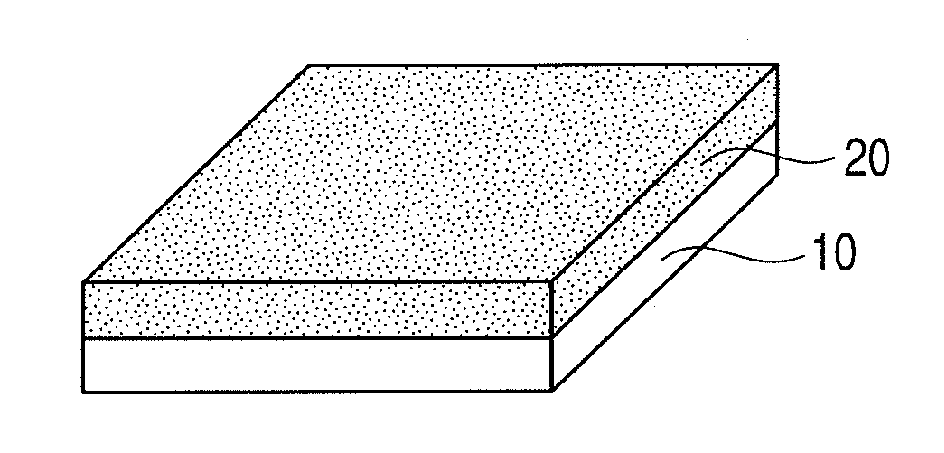
[0053]In FIGS. 1A to 1E, reference numeral 10 denotes a quartz substrate, and reference numeral 20 denotes the base material of a photonic crystal structure formed of an amorphous Si thin film (hereinafter referred to as the Si thin film).

[0054]First, a thin film is formed in a step of preparing a photonic crystal base material, as described below, as the base material...

exemplary embodiment 2

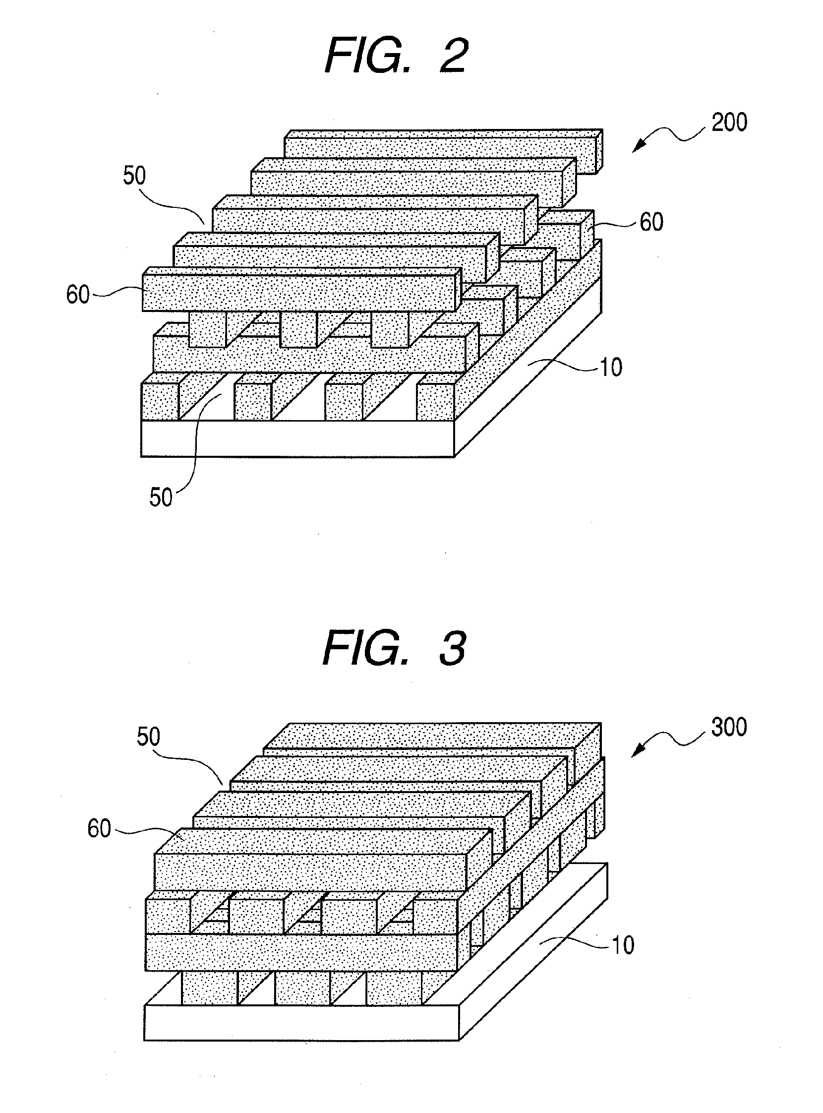
[0059]In exemplary embodiment 2, a description will be made of a constitutional example of a photonic crystal structure to be newly fabricated using the photonic crystal formed in exemplary embodiment 1. Since the present exemplary embodiment is based on a structure basically the same as the photonic crystal structure illustrated in FIG. 2 in the above-described exemplary embodiment of the present invention, FIG. 2 is also used here to describe the present exemplary embodiment. As described with reference to the photonic crystal structure illustrated in FIG. 2 in the above-described exemplary embodiment of the present invention, this photonic crystal is equivalent to the photonic crystal illustrated in FIG. 1E from which the base material part 40 is removed. That is, the rods 60 correspond to the base material part 30 in FIGS. 1A to 1E, and at least one of molecules, atoms and ions different from the constituent element of the base material is arranged in the photonic crystal base m...

exemplary embodiment 3

[0063]In exemplary embodiment 3, a description will be made of a constitutional example of a photonic crystal structure which is newly fabricated using the photonic crystal formed in exemplary embodiment 1 and is different from the photonic crystal structure of exemplary embodiment 2. FIG. 3 illustrates a schematic view used to describe the photonic crystal structure of the present exemplary embodiment. In the present exemplary embodiment, there is used a step which further includes a step of selectively removing the region in which ions have been implanted, following the above-described step of implanting ions. For example, the base material part 30 in FIG. 1E, i.e., a part of Si containing Ga ions, is selectively removed using a solution. Any solutions, including a hydrochloric acid, which dissolve Ga but not Si can be used. First, the photonic crystal structure illustrated in FIG. 1E is placed in the solution and a wait is made until the base material part 30 completely dissolves...


PUM


Abstract

A photonic crystal structure is provided the optical characteristics of which vary periodically in at least one direction, wherein the base material of the photonic crystal structure is formed of a dielectric material, a region containing at least one of molecules, atoms and ions different from the constituent element of the base material is provided in the base material, and the region is arranged in the base material so that the density of one of the molecules, atoms and ions varies periodically in the one direction.

Description

BACKGROUND OF THE INVENTION[0001]1. Field of the Invention[0002]The present invention relates to a photonic crystal structure and a method of manufacturing the photonic crystal structure.[0003]2. Related Background Art[0004]A photonic crystal is a structure in which the refractive indexes of constituent substances are distributed periodically. The photonic crystal is an artificial material capable of realizing novel functions simply by means of structural design. The most noteworthy feature of the photonic crystal is that there is formed therein a so-called photonic band gap, a region through which a specific electromagnetic wave cannot propagate because of the refractive index difference and structural periodicity of constituent materials. When a defect is introduced into the refractive index distribution of the photonic crystal, an energy level (defect level) due to this defect is formed in the photonic band gap. Consequently, the photonic crystal can freely control electromagneti...

Claims


Application Information

Patent Timeline
IPC IPC(8): G02B6/26
CPCB82Y20/00G02B1/005G02B5/1847G02B6/1225
Inventor WANG, SHINANTAMAMORI, KENJIMOTOI, TAIKOOKUNUKI, MASAHIKOONO, HARUHITOAIBA, TOSHIAKI
Owner CANON KK
Why Eureka
Try Eureka