Bi-directional Trimming Methods and Circuits for a Precise Band-Gap Reference
- Summary
- Abstract
- Description
- Claims
- Application Information
AI Technical Summary
Problems solved by technology
Method used
Image
Examples
Embodiment Construction
[0020]The present invention relates to an improvement in trimable bandgap reference circuits. The following description is presented to enable one of ordinary skill in the art to make and use the invention as provided in the context of a particular application and its requirements. Various modifications to the preferred embodiment will be apparent to those with skill in the art, and the general principles defined herein may be applied to other embodiments. Therefore, the present invention is not intended to be limited to the particular embodiments shown and described, but is to be accorded the widest scope consistent with the principles and novel features herein disclosed.
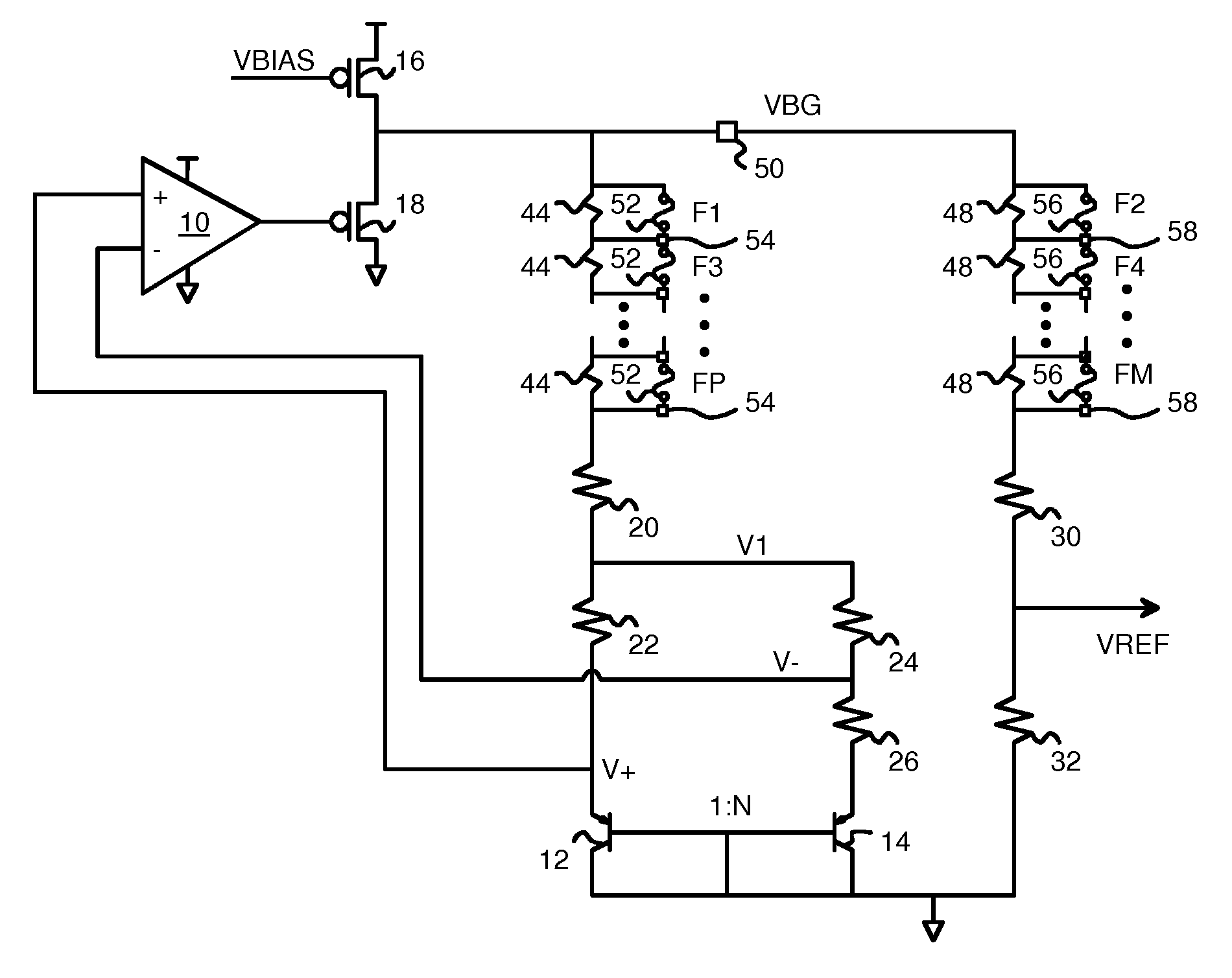
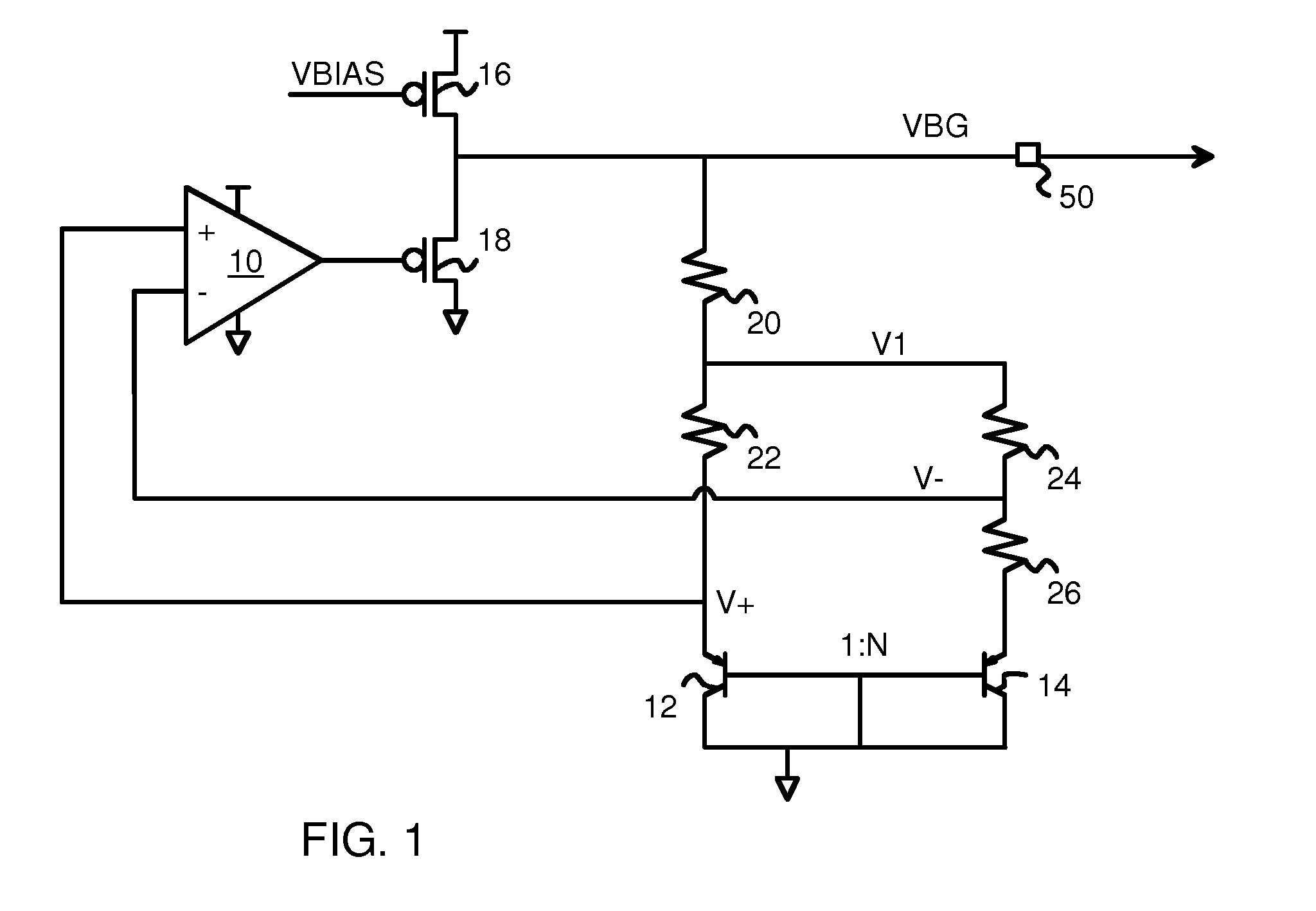
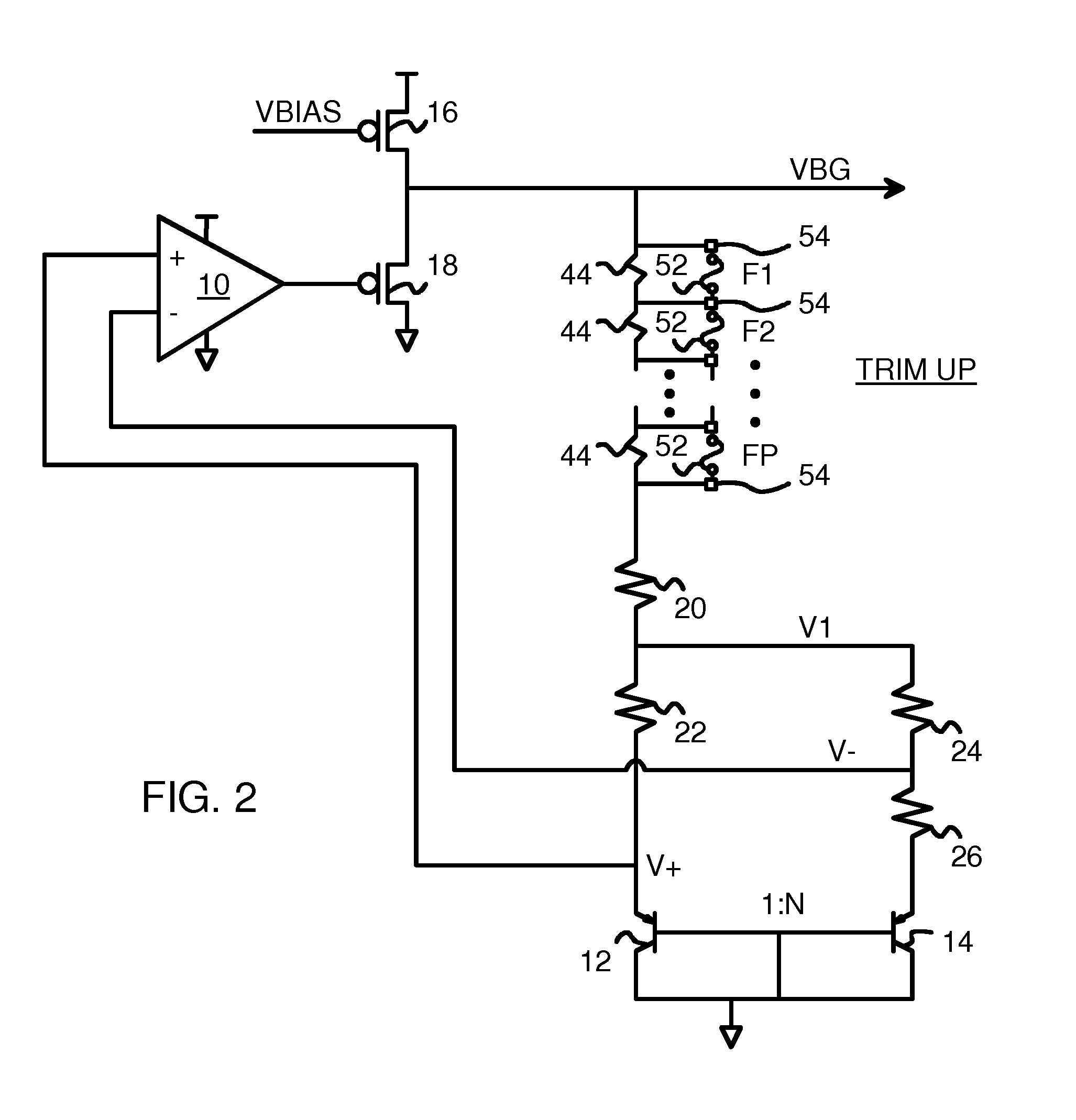
[0021]FIG. 1 is a block diagram of a bandgap reference circuit. PNP transistors 12, 14 have their collectors and their bases tied to ground. PNP transistor 14 is N times larger than PNP transistor 12, and thus sinks about N times more collector current under the same bias conditions.
[0022]A bandgap reference voltag...
PUM
 Abstract
Description
Claims
Application Information


