Multi-field arranging method of LED chips under single lens

a technology of led chips and hemispherical lenses, applied in semiconductor devices for light sources, lighting and heating apparatus, light source combinations, etc., can solve the problems of poor color mixture at the peripheral portion of the hemispherical lens, lack of suitable design, and failure of existing technology for arranging led chips under hemispherical lenses to present flawless light patterns. , to achieve the effect of reducing the overall configuration, maximizing the density of led chips, and improving process and function

Inactive Publication Date: 2011-07-14
HELIO OPTOELECTRONICS
View PDF4 Cites 10 Cited by
  • Summary
  • Abstract
  • Description
  • Claims
  • Application Information

AI Technical Summary

Benefits of technology

One objective of the present invention is to overcome the defects of the light patterns produced by the existing configurations of LED chips under a hemispherical lens, and to provide a new multi-field arranging method of LED chips under a single lens, wherein the technical issue to be addressed is to make each of the LED chips of different colors under the hemispherical lens present a symmetrical light pattern, so as to allow even color mixture, thus being more practical.
Another objective of the present invention is to provide a new multi-field arranging method of LED chips under a single lens, wherein the technical issue to be addressed is to such arrange the LED chips of various colors at a bottom of the single lens that a light pattern formed by mixture of the light of the LED chips is symmetrical from any viewpoint, thereby improving color mixture at the peripheral portion of the single lens, thus being more practical.
Still another objective of the present invention is to provide a new multi-field arranging method of LED chips under a single lens, wherein the technical issue to be addressed is to arrange the LED chips into concentric circles, so as to maximize the density of the LED chips and thereby downsize the overall configuration, thus being more practical.
Since each of LED chips of different colors is allowed to present the symmetrical light pattern, the resultant color mixture can be evener.
The multi-field arranging method helps to maximize the density of the LED chips and thereby downsize the overall configuration.
To sum up, the present invention relates to a multi-field arranging method of LED chips under a single lens, which comprises the steps of: setting a first concentric circle; and arranging at least one first color chip, at least one second color chip and at least one third color chip. The first concentric circle is centered at an axis of a hemispherical lens and formed on a bottom of the hemispherical lens. The color chips are equidistantly arranged in sequence on the first concentric circle, so that all the color chips are allowed to present a symmetrical light pattern under the hemispherical lens, thereby achieving a light field of an evener color mixture. The present invention possessing the above-recited advantageous and practical merits has made significant improvement in both process and function, so as to provide obvious progress to the related technology and produce useful and practical effects. The present invention, as compared with the known configurations of LED chips under a hemispherical lens, has enhanced, outstanding effects, thus being more practical and being exactly a novel, progressive and practical approach.

Problems solved by technology

Thus, polarized light is generated and causes poor color mixture at the peripheral portion of the hemispherical lens 10.
This proves that the existing technology for arranging LED chips under a hemispherical lens still fails to present light patterns that are flawless and convenient to practical applications and needs to be improved.
For remedying these problems, the related manufacturers have long spent every effort to develop solutions, yet a suitable design is still absent.

Method used


Image

  • Multi-field arranging method of LED chips under single lens
  • Multi-field arranging method of LED chips under single lens
  • Multi-field arranging method of LED chips under single lens

Examples


first embodiment

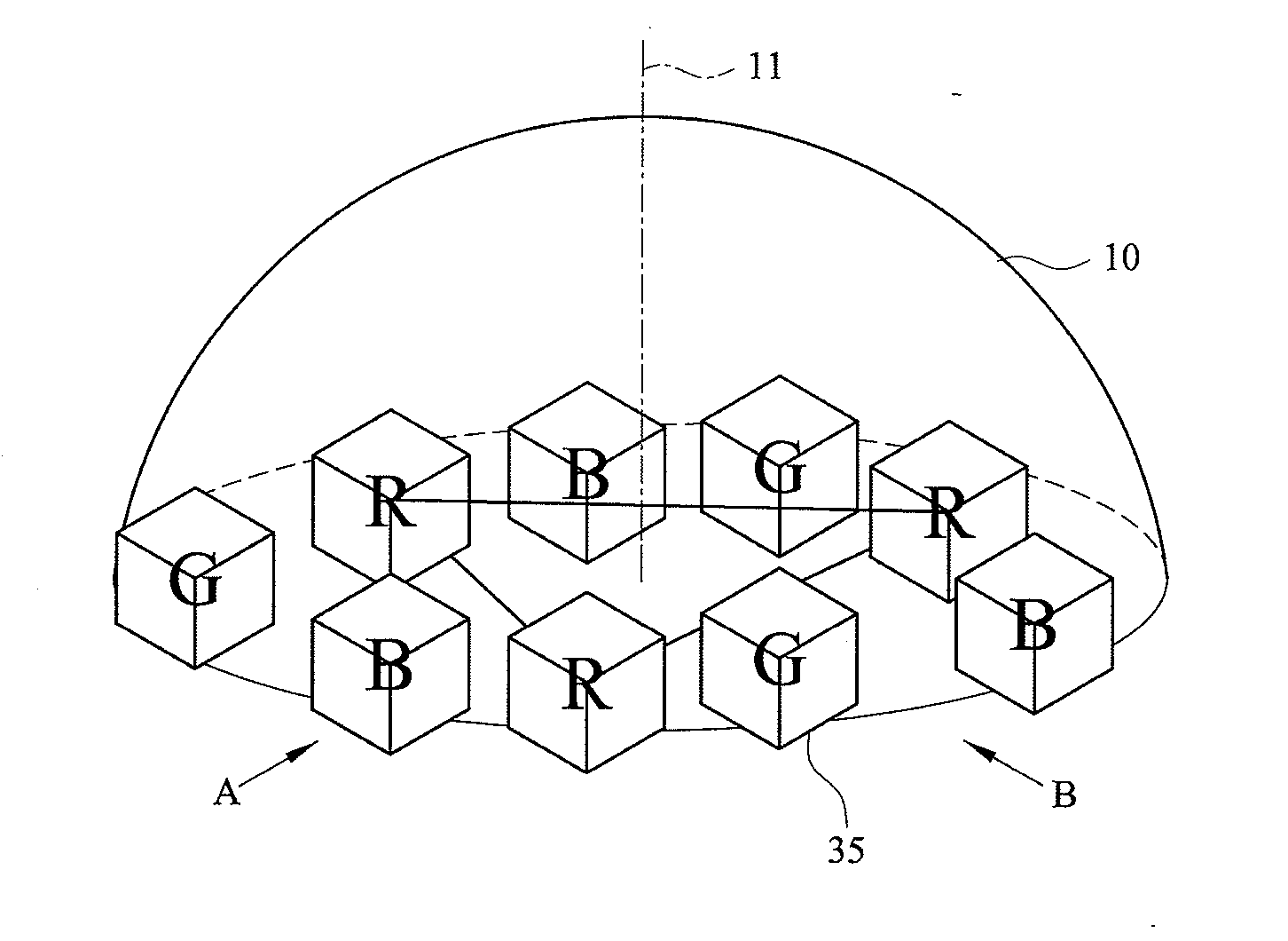
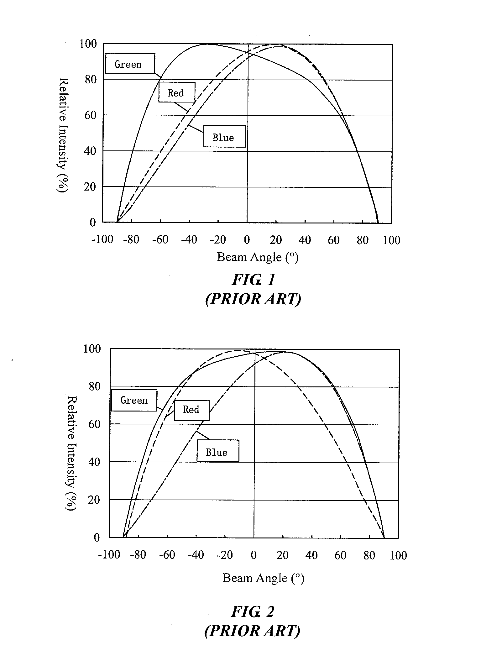
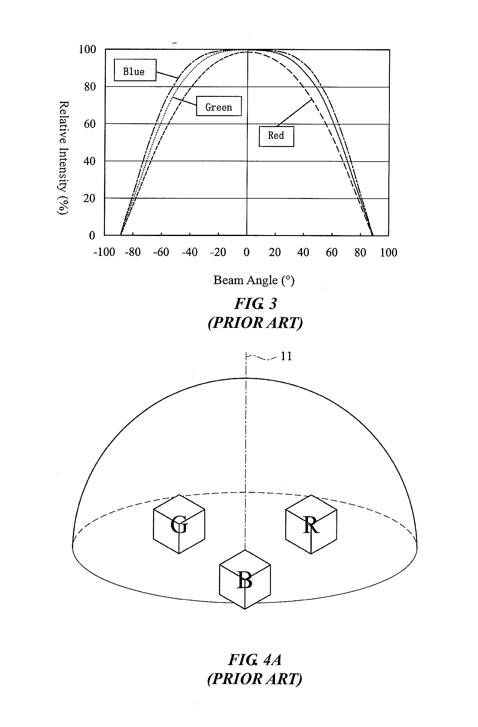
FIG. 5 is a flowchart of a multi-field arranging method S10 of LED chips under a single lens according to a first preferred embodiment of the present invention. FIG. 6 is an exploded view of the LED chips under the single lens according to FIG. 5. FIG. 7 is a first exemplificative arrangement of the LED chips according to the preferred embodiment. FIG. 8A is a perspective view of FIG. 7. FIG. 8B shows a light pattern of the red LED chip of FIG. 7. FIG. 8C is a diagram showing a light intensity profile of the red LED chip from a viewpoint along Arrow A of FIG. 8A. FIG. 8D is a diagram showing a light intensity profile of the red LED chip from a viewpoint along Arrow B of FIG. 8A. FIG. 9 is a second exemplificative arrangement of the LED chips according to the preferred embodiment.

Referring to FIG. 5, the multi-field arranging method S10 according to the first preferred embodiment of the present invention, comprises the steps of: setting a first concentric circle S11; and equidistantl...

second embodiment

FIG. 10 is a flowchart of a multi-field arranging method S10′ of LED chips under a single lens according to a second preferred embodiment of the present invention. FIG. 11 is an exploded view of the LED chips under the single lens according to FIG. 10. FIG. 12 is a third exemplificative arrangement of the LED chips according to the preferred embodiment. FIG. 13 is a fourth exemplificative arrangement of the LED chips according to the preferred embodiment. FIG. 14 is a fifth exemplificative arrangement of the LED chips according to the preferred embodiment.

Referring to FIG. 10, the multi-field arranging method S10′ of the present invention comprises the steps of: setting a first concentric circle S13; arranging a plurality of first color chips S14; setting a second concentric circle S15; and arranging a plurality of second color chips and a plurality of third color chips S16.

In the step of setting a first concentric circle S13, referring to FIG. 11, the first concentric circle 50 is ...

third embodiment

FIG. 15 is a flowchart of a multi-field arranging method S10″ of LED chips under a single lens according to a third preferred embodiment of the present invention. FIG. 16 is an exploded view of the LED chips under the single lens according to FIG. 15. FIG. 17 is a sixth exemplificative arrangement of the LED chips according to the preferred embodiment.

Referring to FIG. 15, the multi-field arranging method S10″ of the present invention comprises the steps of: setting a first color chip S17; setting a first concentric circle S18; and arranging a plurality of second color chips and a plurality of third color chips S19.

In the step of arranging the first color chip S17, referring to FIG. 16, the first color chip 34 is formed on an axis 11 of a hemispherical lens 10. The first color chip 34 may be an LED chip with a relatively large size.

In the step of setting the first concentric circle S18, referring to FIG. 17, the first concentric circle 70 is formed on a bottom of the hemispherical l...


PUM


Abstract

A multi-field arranging method of LED chips under a single lens includes the steps of: setting a first concentric circle on a bottom of a hemispherical lens, wherein the first concentric circle is centered at an axis of the hemispherical lens; and equidistantly arranging at least one first color chip, at least one second color chip and at least one third color chip on the first concentric circle in sequence. The present invention allows the color chips to present symmetrical light patterns through the hemispherical lens, thereby obtaining a light field with evener color mixture.

Description

BACKGROUND OF THE INVENTION1. Technical FieldThe present invention relates to LED arranging methods, and more particularly, to a multi-field arranging method of LED chips under a single lens applicable to color mixture of multiple LED chips.2. Description of Related ArtFIG. 1 is a diagram showing light intensity profiles through a conventional hemispherical lens 10. FIG. 2 is another diagram showing light intensity profiles through the conventional hemispherical lens 10. FIG. 3 is a diagram showing light intensity profiles through a conventional planar lens.FIG. 1 and FIG. 2 are the two diagrams are derived from measuring the light intensity profiles of LED chips of different colors from two different viewpoints through the conventional hemispherical lens 10. According to the diagrams, it is found that since the hemispherical lens 10 has its axis 11 inconsistent with the optical axis of any of the colored LEDs, the resultant light patterns of all the LEDs are asymmetric and varied w...

Claims


Application Information

Patent Timeline
Patent Type & Authority Applications(United States)
IPC IPC(8): H01L33/00
CPCF21K9/00F21Y2105/10F21Y2105/12F21Y2113/13F21Y2115/10
Inventor WANG, CHIH-MINGHO, I-LINWEN, SHIH-YITSENG, PO-MINGLIN, JIUN-MIN
Owner HELIO OPTOELECTRONICS
Why Eureka
Try Eureka