Radiation detector and radiation detection system

a radiation detection and detector technology, applied in the field of radiation detectors and radiation detection systems, can solve the problems of increasing the overall size and weight of the detector, increasing the size and thickness of the sensor panel, and increasing the structure for protecting the peripheral circuitry from radiation, so as to reduce the amount of radiation incident and reduce damage to the peripheral circuitry

Inactive Publication Date: 2011-08-18
CANON KK
View PDF7 Cites 30 Cited by
  • Summary
  • Abstract
  • Description
  • Claims
  • Application Information

AI Technical Summary

Benefits of technology

[0009]In accordance with the present invention, the sealing resin sealing the scintillator layer can reduce the amount of radiation incident on the peripheral circuitry, protect the scintillator from changes in environmental conditions and reduce damage to the peripheral circuitry without the installation of another radiation-shielding member.

Problems solved by technology

These protective layers prevent the intrusion of water and other foreign substances into the scintillator layer, but tend to increase the overall size and weight of the detector.
In the radiation detector according to Japanese Patent Laid-Open No. 2004-177217, however, the structures for protecting the peripheral circuitry from radiation increase the size and thickness of a sensor panel.

Method used


Image

  • Radiation detector and radiation detection system
  • Radiation detector and radiation detection system
  • Radiation detector and radiation detection system

Examples


first embodiment

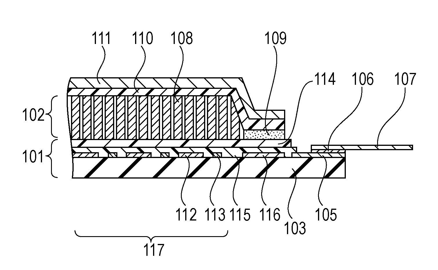
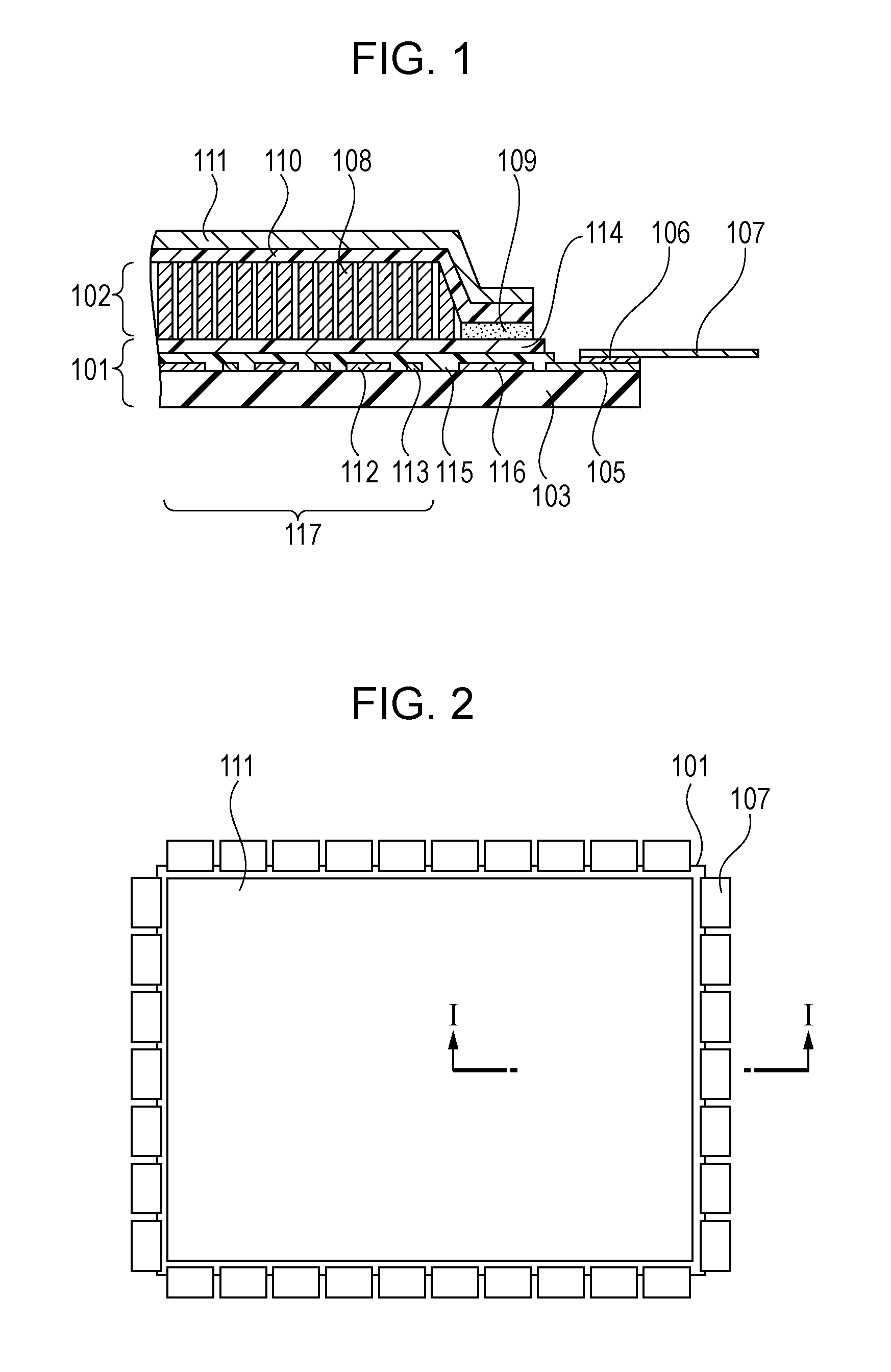
[0020]FIG. 2 is a plan view of a radiation detector according to a first embodiment of the present invention. FIG. 1 is a cross-sectional view taken along the line I-I in FIG. 2. FIG. 3 is a plan view of the sensor panel illustrated in FIGS. 1 and 2. Like reference numerals designate like parts throughout these figures.

[0021]As illustrated in FIG. 1, a sensor panel 101 includes photoelectric conversion elements 112 and TFT's (not shown) formed of a semiconductor film on an insulating substrate 103, for example, formed of glass or resin. The photoelectric conversion elements 112 or the TFT's are connected to wires 113. The photoelectric conversion elements 112 and the wires 113 are two-dimensionally arranged to form a photodetector 117. Peripheral circuitry 116 processes (for example, amplifies) signals sent from the photoelectric conversion elements 112 through wires 113. As illustrated in FIG. 3, the peripheral circuitry 116 is disposed on the periphery of the photodetector 117.

[00...

second embodiment

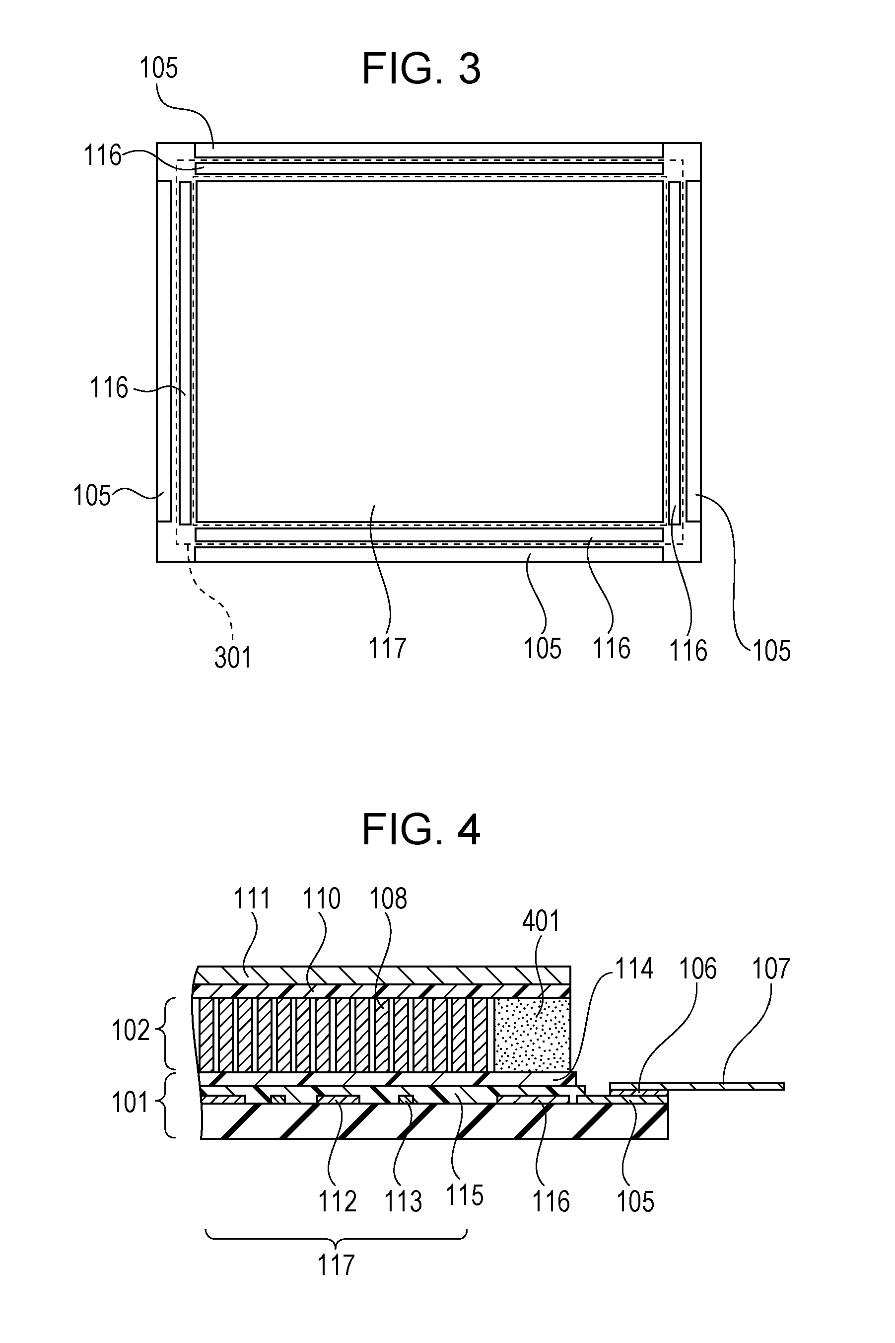
[0044]FIG. 4 is a cross-sectional view of a radiation detector according to a second embodiment of the present invention. In FIG. 4, the same parts as in FIG. 1 are denoted by the same reference numerals and will not be further described. The plan view of the radiation detector according to the second embodiment is the same as FIG. 2. A sensor panel of the radiation detector is the same as the sensor panel illustrated in FIG. 3.

[0045]A sealing resin 401 in the present embodiment has substantially the same thickness as the scintillator layer 102. The sealing resin 401 can therefore more easily shield radiation than the first embodiment. In the first embodiment, the sensor panel 101 is bonded to the scintillator protection layer 110 with the sealing resin 109. In the present embodiment, after a structure formed of the sealing resin 401 is formed on the periphery of the scintillator layer 102, the scintillator protection layer 110 is formed on the scintillator layer 102 and the sealing...

third embodiment

[0046]FIG. 5 is a cross-sectional view of a radiation detector according to a third embodiment of the present invention. In FIG. 5, the same parts as in FIG. 1 are denoted by the same reference numerals and will not be further described.

[0047]In the present embodiment, the scintillator layer 102 is not directly formed on the sensor panel 101 but is formed on a substrate 502 formed of a reflective material. A reflective-layer-protection layer 503 is formed on the substrate 502. A scintillator layer 102 containing columnar crystals 108 is formed on the reflective-layer-protection layer 503. A scintillator protection layer 504 is formed on the scintillator layer 102, thus constituting a scintillator substrate 506. The scintillator substrate 506 is bonded to the sensor panel 101 such that the scintillator layer 102 is disposed within. The scintillator layer 102 is sealed with a sealing resin 501 between the sensor panel 101 and the substrate 502. In other words, the substrate 502 consti...


PUM


Abstract

A radiation detector includes a sensor panel including a photodetector and peripheral circuitry, the photodetector includes a two-dimensional array of photoelectric conversion elements arranged on a substrate, the peripheral circuitry is electrically connected to the photoelectric conversion elements and is disposed on the periphery of the photodetector; a scintillator layer is disposed on the photodetector of the sensor panel, the scintillator layer converts radiation into light that is detectable by the photoelectric conversion elements; a scintillator protection member covers the scintillator layer; and a sealing resin seals the scintillator layer, the sealing resin is disposed between the sensor panel and the scintillator protection member on the periphery of the scintillator layer; the sealing resin is disposed on top of the peripheral circuitry; and particles containing a radiation-absorbing material are dispersed in the sealing resin.

Description

BACKGROUND OF THE INVENTION[0001]1. Field of the Invention[0002]The present invention relates to a radiation detector and a radiation detection system for use in medical diagnostic equipment, nondestructive testing equipment, and other equipment; more particularly, the preset invention relates to a radiation detector and a radiation detection system for use in digital radiography.[0003]2. Description of the Related Art[0004]X-ray film systems generally used for X-ray photography employ a fluorescent screen containing an X-ray fluorescent layer and a film. Digital radiation detectors that include a scintillator layer and a two-dimensional photodetector are also being used and can potentially replace the use of X-ray film systems. The scintillator layer functions as a wavelength converter that can convert X-rays into visible light; and the two-dimensional photodetector converts the visible light into an electric signal which can be digitally processed. Accordingly, the two-dimensional...

Claims


Application Information

Patent Timeline
Patent Type & Authority Applications(United States)
IPC IPC(8): G01T1/208
CPCG01T1/202
Inventor ISHIDA, YOHEIOKADA, SATOSHINAGANO, KAZUMINOMURA, KEIICHISASAKI, YOSHITO
Owner CANON KK
Why Eureka
Try Eureka