Organic light emitting display device

a light-emitting display and organic technology, applied in the field of organic light-emitting display devices, can solve the problem of not being able to sufficiently compensate the threshold voltage of the driving transistor

Active Publication Date: 2011-08-18
SAMSUNG DISPLAY CO LTD
View PDF7 Cites 55 Cited by
  • Summary
  • Abstract
  • Description
  • Claims
  • Application Information

AI Technical Summary

Benefits of technology

[0029]In embodiments of an organic light emitting display device according to the present invention, the threshold voltage of a driving transistor can be compensated during a period of 2H or wider. Accordingly, an image with a desired luminance can be displayed even in fast driving. Further, the degradation of an OLED can be compensated using a compensator. Accordingly, an image with a desired luminance can be displayed regardless of the degradation of the OLED.

Problems solved by technology

Therefore, it is not possible to sufficiently compensate the threshold voltage of the driving transistor.

Method used


Image

  • Organic light emitting display device
  • Organic light emitting display device
  • Organic light emitting display device

Examples


Embodiment Construction

[0041]Hereinafter, certain exemplary embodiments according to the present invention will be described with reference to the accompanying drawings. Here, when a first element is described as being coupled to a second element, the first element may be not only directly coupled (for example, connected) to the second element but may also be indirectly coupled (for example, electrically connected) to the second element via one or more third elements. Further, some of the elements that are not essential to the complete understanding of the exemplary embodiments of the invention are omitted for clarity. In addition, like reference numerals refer to like elements throughout. Finally, reference names for power sources and their corresponding voltages are used interchangeably, with the appropriate meaning apparent from context.

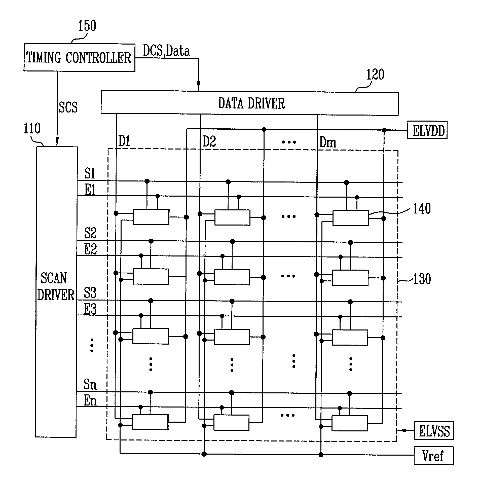
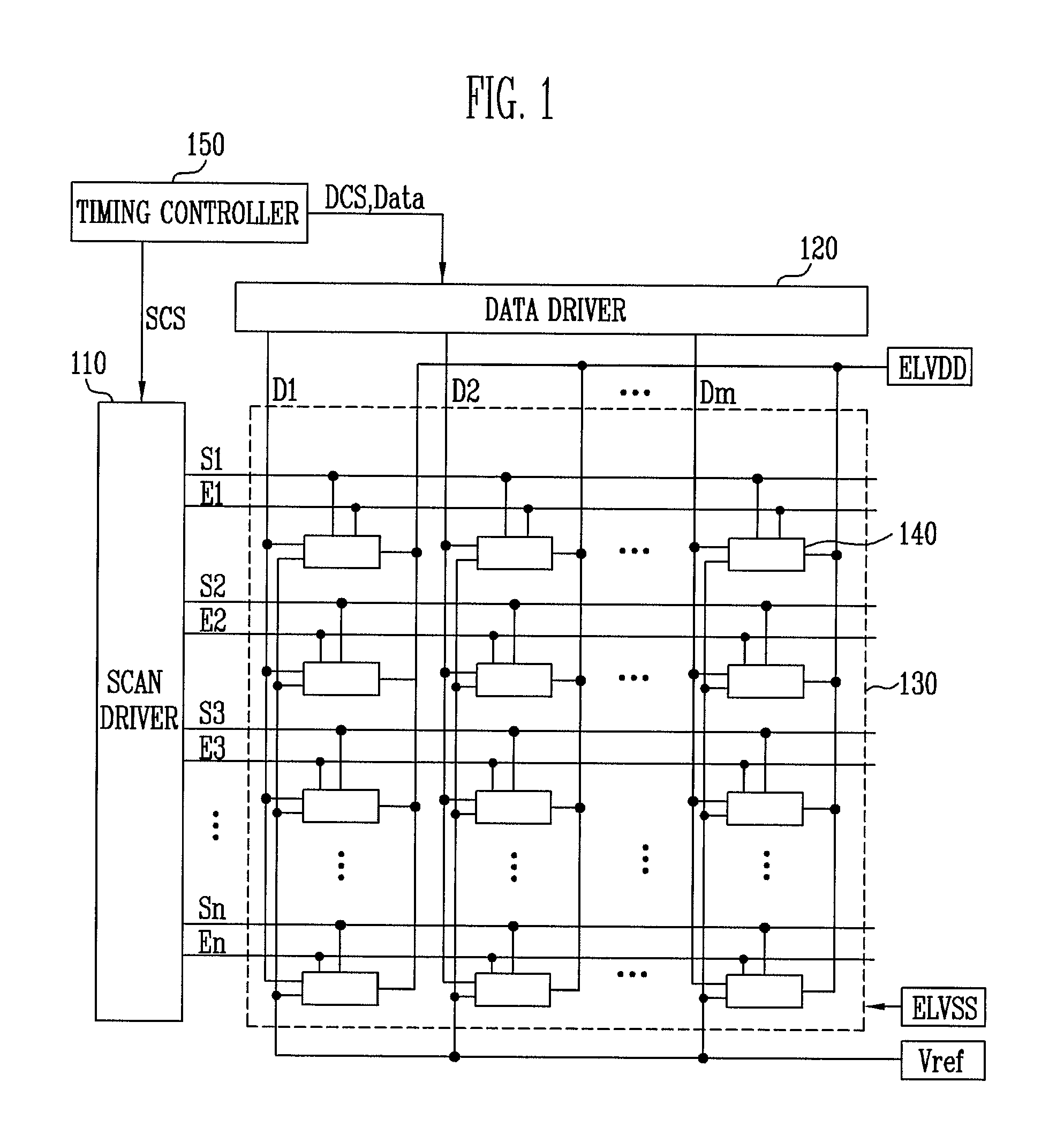
[0042]FIG. 1 is a block diagram of an organic light emitting display device according to an embodiment of the present invention.

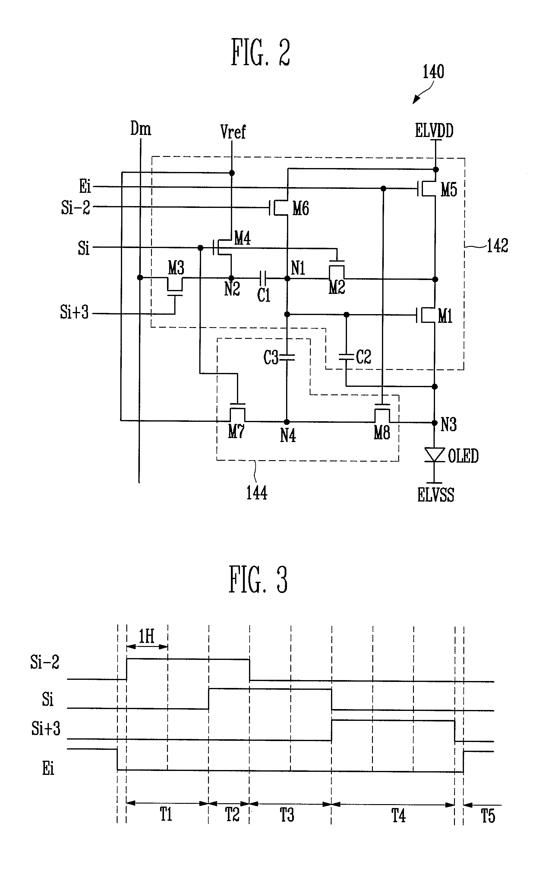
[0043]Referring to FIG. 1, the organic l...


PUM


Abstract

An organic light emitting display device includes a scan driver, a data driver, and pixels. The scan driver is for sequentially supplying, during each horizontal period of a width 1H, a scan signal with a width of at least 2H to scan lines. The scan driver is further for sequentially supplying an emission control signal to emission control lines that are substantially parallel to the scan lines. The data driver supplies data signals to data lines. Each pixel includes an organic light emitting diode (OLED), a pixel circuit having a first transistor for controlling the amount of current supplied to the OLED, and a compensator for controlling the voltage of a gate electrode of the first transistor for compensating a degradation of the OLED. The compensator includes two transistors and a capacitor. One transistor is coupled to a scan line, and the other is coupled to an emission control line.

Description

CROSS-REFERENCE TO RELATED APPLICATION[0001]This application claims priority to and the benefit of Korean Patent Application No. 10-2010-0014111, filed in the Korean Intellectual Property Office on Feb. 17, 2010, the entire content of which is incorporated herein by reference.BACKGROUND[0002]1. Field[0003]Aspects of embodiments according to the present invention relate to an organic light emitting display device.[0004]2. Description of Related Art[0005]Recently, there have been developed various types of flat panel display devices having less weight and volume than that of a comparable cathode ray tube device. The flat panel display devices include liquid crystal display devices, field emission display devices, plasma display panels, organic light emitting display devices, and the like.[0006]Among these flat panel display devices, the organic light emitting display device displays images using organic light emitting diodes (OLEDs) that emit light through recombination of electrons a...

Claims


Application Information

Patent Timeline
Patent Type & Authority Applications(United States)
IPC IPC(8): G09G5/00G09G3/30
CPCG09G3/3233G09G2300/0819G09G2300/0852G09G2320/045G09G2310/0262G09G2320/043G09G2300/0861
Inventor CHUNG, BO-YONGPARK, YONG-SUNG
Owner SAMSUNG DISPLAY CO LTD
Why Eureka
Try Eureka