

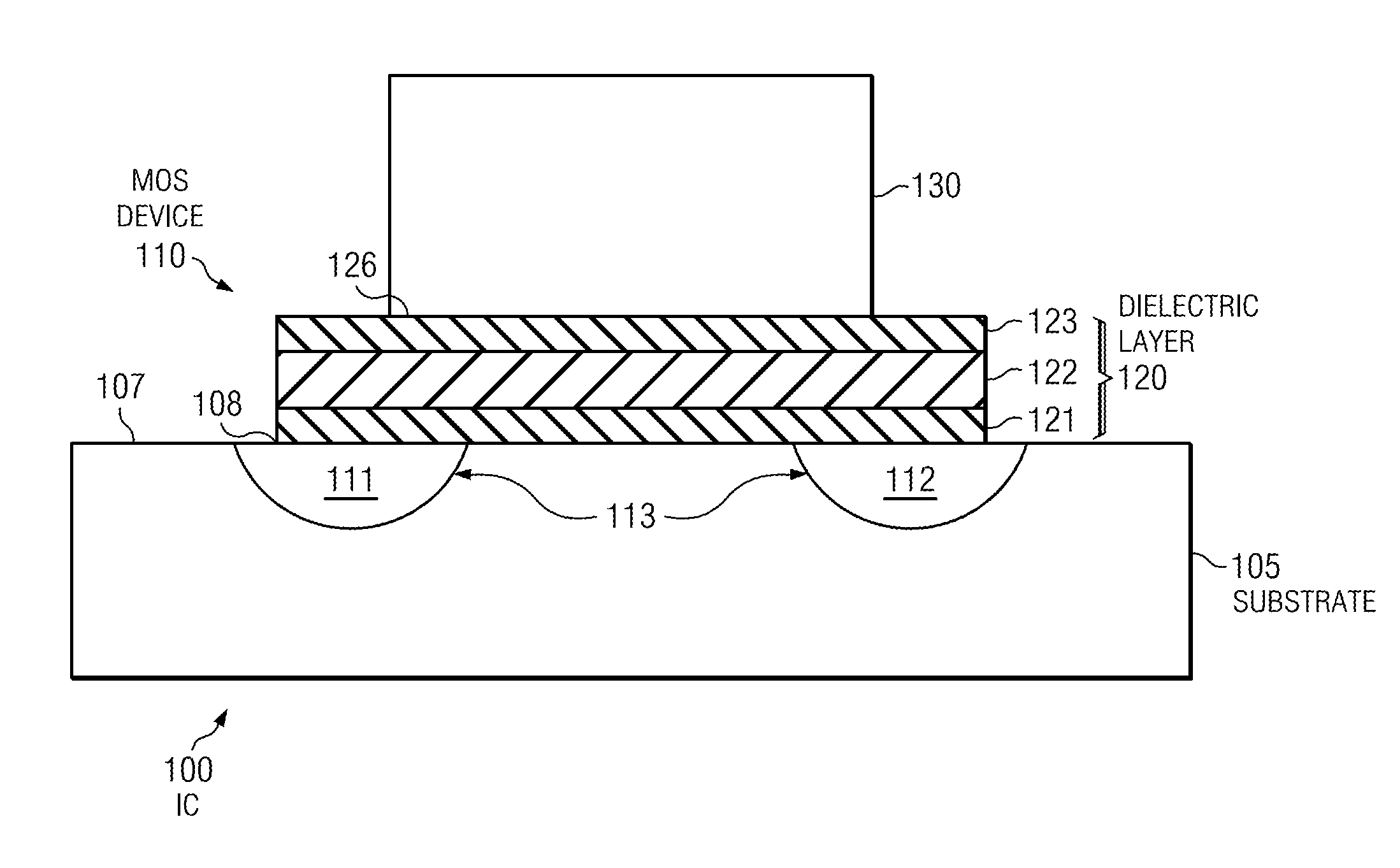
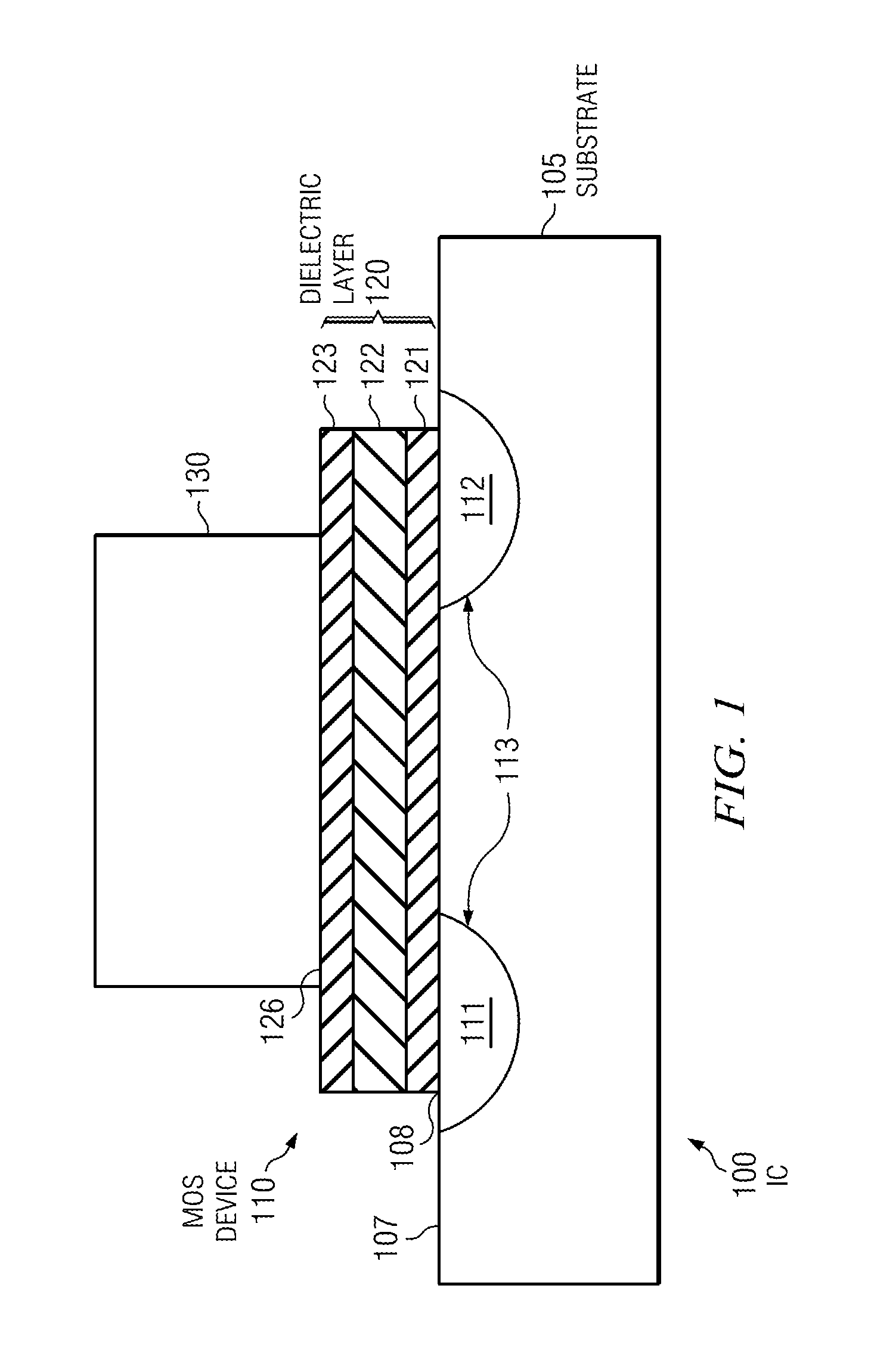
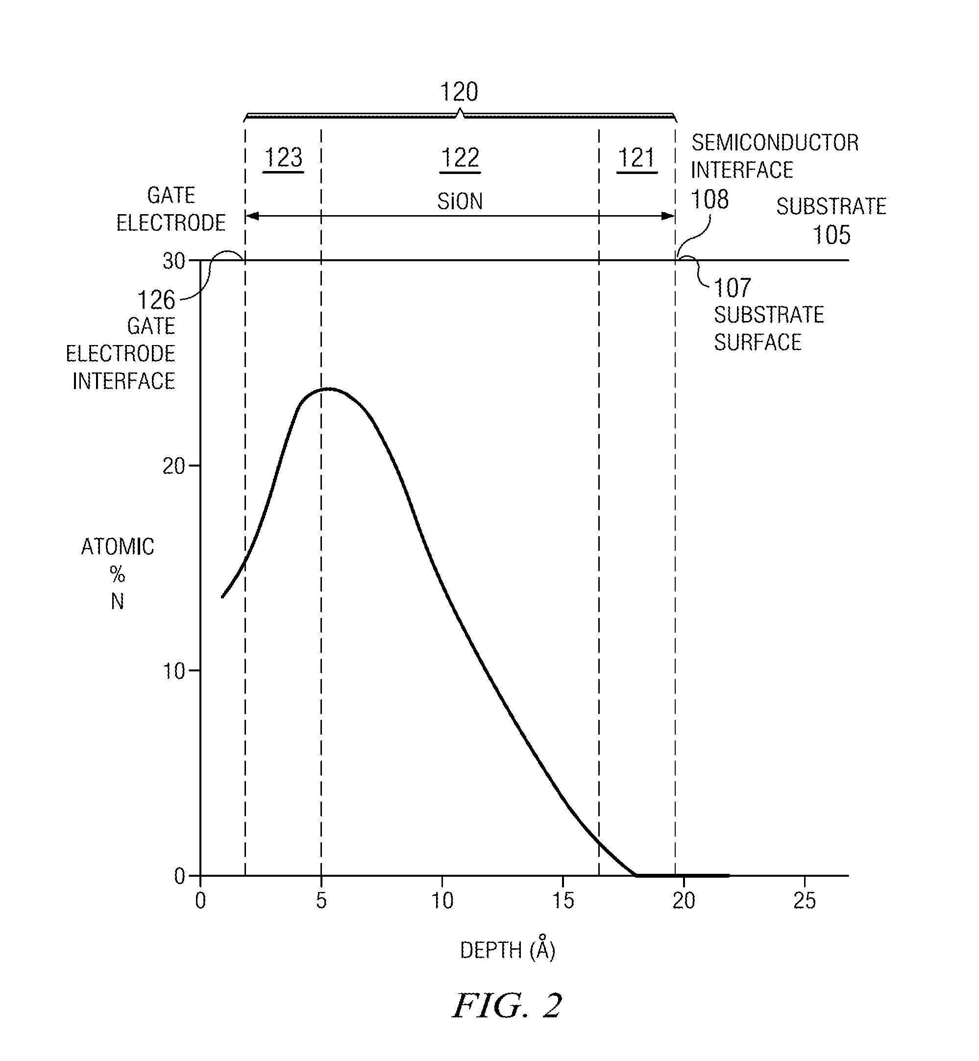
Semiconductor device including sion gate dielectric with portions having different nitrogen concentrations
a technology of sion gate dielectric and dielectric layer, which is applied in the direction of semiconductor devices, transistors, electrical devices, etc., can solve the problems of limited n that can be incorporated into the bulk of the sion layer, and achieve the effects of reducing b deactivation, minimizing poly depletion, and minimizing leakag
- Summary
- Abstract
- Description
- Claims
- Application Information
AI Technical Summary
Benefits of technology
Problems solved by technology
Method used
Image

Examples
examples
[0027]Disclosed embodiments are further illustrated by the following specific Examples, which should not be construed as limiting the scope or content of embodiments disclosed herein in any way.
[0028]FIG. 4 a plot of gate leakage density (Jg (A / cm2)) versus inversion electrical thickness (Tox, inv (A)) for a SiON gate dielectric layer formed using a 2-step PNA compared to a SiON gate dielectric layer formed using a conventional single step N2 / O2 PNA, according to a disclosed embodiment. It can be seen that the 2-Step PNA described herein (inert anneal followed by an oxidizing anneal) results in superior Jg / Tox,inv and Ion / Ioff performance as compared to the single step N2 / O2 PNA (shown as “Prior Art”).
[0029]While various embodiments of the invention have been described above, it should be understood that they have been presented by way of example only, and not limitation. Numerous changes to the disclosed embodiments can be made in accordance with the disclosure herein without depar...
PUM
 Abstract
Description
Claims
Application Information