Video processing circuit, video processing method, liquid crystal display device, and electronic apparatus

a video processing circuit and liquid crystal display technology, applied in the field of video processing circuits, video processing methods, liquid crystal display devices, electronic devices, can solve the problems of reducing the aperture ratio, unable to apply the technique to an existent liquid crystal panel which has been manufactured, and the display defect is likely to be reduced. the effect of reducing the reverse tilt domain

Active Publication Date: 2011-08-25
SEIKO EPSON CORP
View PDF2 Cites 21 Cited by
  • Summary
  • Abstract
  • Description
  • Claims
  • Application Information

AI Technical Summary

Benefits of technology

[0008]An advantage of some aspects of the invention is to provide a technique for reducing reverse tilt domains while eliminating these drawbacks.

Problems solved by technology

For example, when a lateral electric field is applied to liquid crystal which should be driven by a vertical electric field as in the vertical alignment (VA) mode or the twisted nematic (TN) mode, an alignment defect of liquid crystal (that is, reverse tilt domain) occurs, causing a display defect.
However, the technique for reducing the reverse tilt domains with the structure of the liquid crystal panel has such drawbacks that the aperture ratio is likely t decrease, and that the technique cannot be applied to an existent liquid crystal panel which has been manufactured without devising its structure.
On the other hand, the technique for clipping a video signal having a set value or more has such a drawback that the brightness of an image to be displayed is limited to the set value.

Method used


Image

  • Video processing circuit, video processing method, liquid crystal display device, and electronic apparatus
  • Video processing circuit, video processing method, liquid crystal display device, and electronic apparatus
  • Video processing circuit, video processing method, liquid crystal display device, and electronic apparatus

Examples


first embodiment

[0031]A first embodiment of the invention will be described.

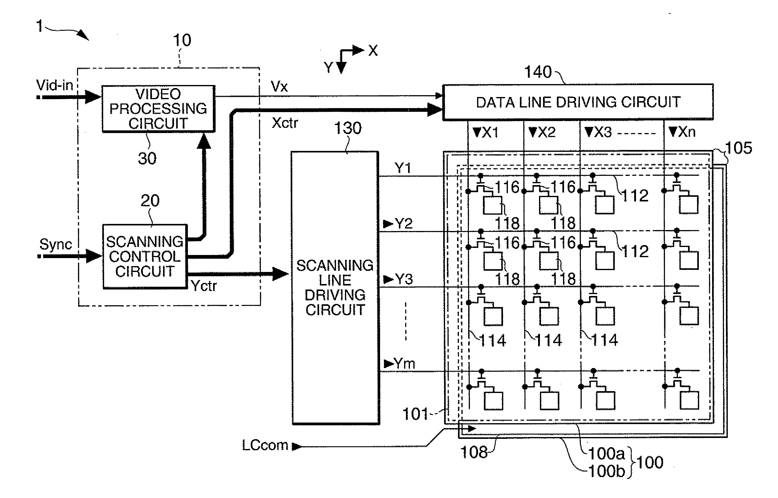
[0032]FIG. 1 is a block diagram showing the overall configuration of a liquid crystal display device to which a video processing circuit according to the embodiment is applied.

[0033]As shown in FIG. 1, the liquid crystal display device 1 has a control circuit 10, a liquid crystal panel 100, a scanning line driving circuit 130, and a data line driving circuit 140. To the control circuit 10, a video signal Vid-in is supplied from a higher-level device in synchronization with a synchronizing signal Sync. The video signal Vid-in is digital data which specifies a gray-scale level of each pixel in the liquid crystal panel 100, and is supplied in a scanning order according to a vertical scanning signal, a horizontal scanning signal, and a dot clock signal (all not shown) included in the synchronizing signal Sync.

[0034]Although the video signal Vid-in specifies a gray-scale level, it can safely be said that the video signal Vid-in ...

second embodiment

[0087]Next, a second embodiment of the invention will be described.

[0088]In the following description, the same components as those of the first embodiment are denoted by the same reference numerals, and the description thereof is appropriately omitted.

[0089]In the first embodiment, by analyzing the video signal Vid-in, when a dark pixel and a bright pixel are next to each other, the gray-scale level of a pixel group whose applied voltage is higher is corrected. Contrary to this, for further reducing a lateral electric field, an applied voltage to a pixel whose applied voltage is lower, that is, a pixel which is likely to be affected by an electric field (dark pixel in the normally black mode), may be increased.

[0090]FIG. 8 is a block diagram showing the configuration of the video processing circuit 30 according to the second embodiment.

[0091]The configuration of the video processing circuit 30 of the second embodiment differs from that of the first embodiment in that a calculation ...

third embodiment

[0101]Next, a third embodiment of the invention will be described.

[0102]In the following description, the same components as those of the first and second embodiments are denoted by the same reference numerals, and the detailed description thereof is appropriately omitted.

[0103]A specific example of a correction process by the video processing circuit 30 of the third embodiment will be described with reference to FIGS. 11A to 13B. In each of FIGS. 11A to 13B, each rectangle corresponds to one pixel, and an alphabet or a combination of alphabet and numerical value, shown inside the rectangle, corresponds to each gray-scale level. P1 to P12 are reference numerals for identifying respective pixels, and the numeric suffix is incremented from the left to the right in the drawing. In the graph below the rectangles, the horizontal axis represents the position of each pixel, while the vertical axis represents an applied voltage to a liquid crystal element corresponding to a pixel at each pi...


PUM


Abstract

A video processing circuit for a liquid crystal panel, includes: a boundary detecting unit which detects a boundary between a first pixel whose applied voltage specified by an input video signal is below a first voltage and a second pixel whose applied voltage is equal to or higher than a second voltage which is higher than the first voltage; and a correction unit which corrects, for at least two second pixels one of which is adjacent to the boundary detected by the boundary detecting unit on the opposite side of the first pixel and which are successive in a direction opposite to the boundary, an applied voltage to liquid crystal elements corresponding to the second pixels from the applied voltage specified by the video signal to a voltage which is equal to or higher than the first voltage and below the second voltage.

Description

BACKGROUND[0001]1. Technical Field[0002]The present invention relates to a technique for reducing display defects in a liquid crystal panel.[0003]2. Related Art[0004]Liquid crystal panels each have a configuration in which liquid crystal is interposed between a pair of substrates with a given gap. Specifically, the liquid crystal panel has pixel electrodes arranged in matrix and each disposed corresponding to each of pixels in one of the substrates and a common electrode disposed in common for the pixels in the other substrate, and the liquid crystal is interposed between the pixel electrodes and the common electrode. When a voltage according to a gray-scale level is applied and held between the pixel electrode and the common electrode, the alignment state of the liquid crystal is defined for each pixel, whereby the transmittance or reflectance is controlled. Accordingly, it can be said in the configuration that only a component in a direction from the pixel electrode toward the com...

Claims


Application Information

Patent Timeline
Patent Type & Authority Applications(United States)
IPC IPC(8): H04N5/21
CPCG09G3/2096G09G2370/08G09G2320/0209G09G3/3648
Inventor IISAKA, HIDEHITOHOSAKA, HIROYUKI
Owner SEIKO EPSON CORP
Why Eureka
Try Eureka