Video processing circuit, video processing method, liquid crystal display device, and electronic apparatus

a video processing circuit and video processing method technology, applied in the direction of instruments, television systems, static indicating devices, etc., can solve the problems of display defects, the effect of an electric field generated between the adjacent pixel electrodes, and the effect of an electric field in the direction parallel (horizontal) to the substrate surface becoming unignorable, and the aperture ratio is likely to decrease. , to achieve the effect of reducing the reverse tilt domain

Active Publication Date: 2014-10-28
SEIKO EPSON CORP
View PDF29 Cites 0 Cited by
  • Summary
  • Abstract
  • Description
  • Claims
  • Application Information

AI Technical Summary

Benefits of technology

[0008]An advantage of some aspects of the invention is that it provides a technique of reducing reverse tilt domain while solving these drawbacks.
[0010]In the video processing circuit, it is preferable that the correction portion corrects the applied voltages to liquid crystal devices corresponding to the first pixel adjacent to the risk boundary and one or more first pixels continuous to the first pixel from the applied voltage specified by the video signal to the third voltage or higher. Moreover, it is preferable that, when a refresh time interval of the display of the liquid crystal panel is S and a response time of the liquid crystal device when the applied voltage is changed from a voltage lower than the third voltage to the voltage corrected by the correction portion is T1, if S<T1, the number of first pixels of which the applied voltage is to be corrected is determined by the value of an integer part of a division of the response time T1 by the time interval S. According to this configuration, it is possible to prevent the occurrence of reverse tilt domain even when the response time of a liquid crystal device is longer than the refresh time interval of the display screen. Specifically, when the refresh time interval of the display of the liquid crystal panel is S and the response time of the liquid crystal device when the applied voltage is changed to the correction voltage is T1, if S<T1, the number of first pixels of which the applied voltage is to be corrected may be determined by the value of an integer part of a division of the response time T1 by the time interval S.
[0012]In the video processing circuit, it is preferable that the correction portion corrects the applied voltages to liquid crystal devices corresponding to the second pixel adjacent to the risk boundary and one or more second pixels continuous to the second pixel from the applied voltage specified by the video signal to a voltage lower than the second voltage and higher than the first voltage. It is also preferable that, when a refresh time interval of the display of the liquid crystal panel is S and a response time of the liquid crystal device when the applied voltage is changed from a voltage higher than the second voltage to the voltage corrected by the correction portion is TI, if S<T1, the number of second pixels of which the applied voltage is to be corrected is determined by the value of an integer part of a division of the response time T1 by the time interval S. According to this configuration, it is possible to prevent the occurrence of reverse tilt domain even when the response time of a liquid crystal device is longer than the refresh time interval of the display screen. Specifically, when the refresh time interval of the display of the liquid crystal panel is S and the response time of the liquid crystal device when the applied voltage is changed to the correction voltage is T, if S<T, the number of second pixels of which the applied voltage is to be corrected may be determined by the value of an integer part of a division of the response time T by the time interval S.
[0013]In the video processing circuit, it is preferable that the correction portion corrects an applied voltage to a liquid crystal device corresponding to a first pixel which is adjacent to the risk boundary from the applied voltage specified by the input video signal to a voltage equal to or higher than the third voltage and lower than the second voltage when the applied voltage specified by the video signal input to the first pixel is lower than the third voltage lower than the first voltage. With this configuration, the difference in the applied voltage between the adjacent pixels is further decreased, and the occurrence of reverse tilt domain can be suppressed more effectively.
[0014]In the video processing circuit, it is preferable that the correction portion corrects the applied voltages to liquid crystal devices corresponding to the first pixel adjacent to the risk boundary and one or more first pixels continuous to the first pixel from the applied voltage specified by the video signal to a voltage equal to or higher than the third voltage and lower than the second voltage. It is also preferable that, when a refresh time interval of the display of the liquid crystal panel is S and a response time of the liquid crystal device when the applied voltages to the liquid crystal devices corresponding to the first pixels are changed from a voltage lower than the third voltage to the voltage corrected by the correction portion is T2, if S<T2, the number of first pixels of which the applied voltage is to be corrected is determined by the value of an integer part of a division of the response time T2 by the time interval S. With this configuration, the difference in the applied voltage between the adjacent pixels is further decreased, and the occurrence of reverse tilt domain can be suppressed more effectively. Moreover, it is possible to prevent the occurrence of reverse tilt domain even when the response time of a liquid crystal device is longer than the refresh time interval of the display screen.
[0015]In the video processing circuit, it is preferable that the correction portion corrects the applied voltage to the liquid crystal device corresponding to the first pixel subjected to the correction to a voltage that gives an initial tilt angle to the liquid crystal device. According to this configuration, it is possible to suppress the liquid crystal molecules from entering a reverse tilt state while suppressing a change in the transmittance of a dark pixel.

Problems solved by technology

However, as the pixel pitch has narrowed with further miniaturization and higher definition in recent years, the effect of an electric field which is generated between the adjacent pixel electrodes, namely an electric field in the direction parallel (horizontal) to the substrate surface has become unignorable.
For example, when a horizontal electric field is applied to a liquid crystal that is designed to be driven by a vertical electric field such as in a VA (Vertical Alignment) or TN (Twisted Nematic)-mode liquid crystal, there is a problem in that alignment defects (namely, reverse tilt domain) occur in the liquid crystal, thus causing display defects.
However, the technique of reducing the reverse tilt domain by devising a new liquid crystal panel structure has a drawback in that the aperture ratio is likely to decrease and it is difficult to apply the technique to a liquid crystal panel which is not manufactured in advance so as to have the new structure.
On the other hand, the technique of clipping away the video signals having a luminance value equal to or higher than a preset value has a drawback in that the brightness of displayed images is limited to the preset value.

Method used


Image

  • Video processing circuit, video processing method, liquid crystal display device, and electronic apparatus
  • Video processing circuit, video processing method, liquid crystal display device, and electronic apparatus
  • Video processing circuit, video processing method, liquid crystal display device, and electronic apparatus

Examples


first embodiment

[0045]First, a first embodiment of the invention will be described.

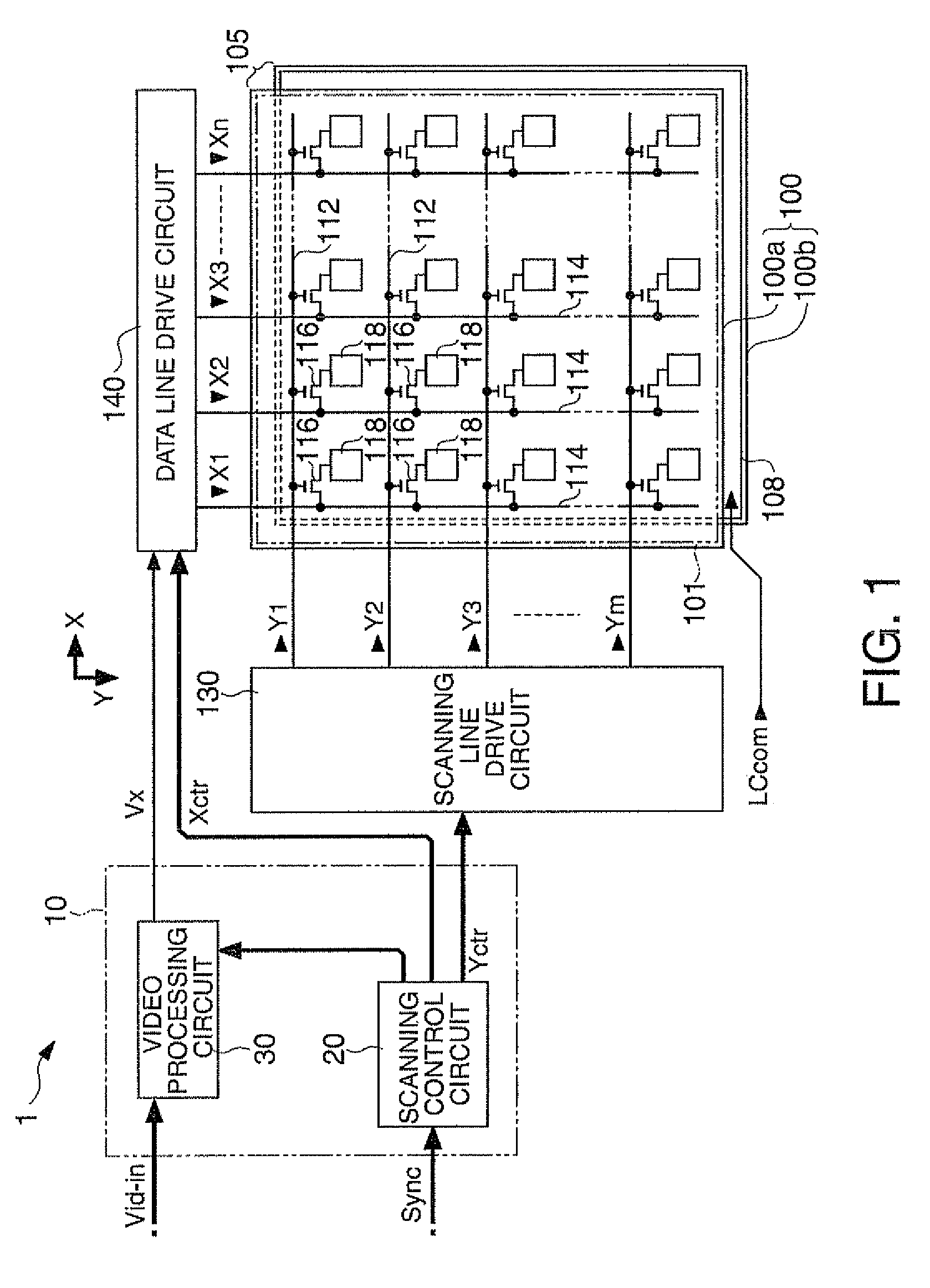
[0046]FIG. 1 is a block diagram showing an overall configuration of a liquid crystal display device having a video processing circuit according to this embodiment,

[0047]As shown in FIG. 1, a liquid crystal display device 1 includes a control circuit 10, a liquid crystal panel 100, a scanning line drive circuit 130, and a data line drive circuit 140. A video signal Vid-in is supplied from a high-order device to the control circuit 10 in synchronization with a synchronization signal Sync. The video signal Vid-in is digital data that specifies the gradation levels of the respective pixels in the liquid crystal panel 100 and is supplied in the scanning order based on the vertical / horizontal scanning signals and dot clock signal (not shown) included in the synchronization signal Sync.

[0048]Although the video signal Vid-in specifies the gradation level, since the applied voltage to a liquid crystal device is determined by ...

second embodiment

[0151]Next, a second embodiment of the invention will be described. In this embodiment, it is also assumed that the liquid crystal device operates in the normally black mode. This applies to the following embodiments unless stated otherwise. Moreover, in the following description, the same configurations as in the first embodiment will be denoted by the same reference numerals, and detailed description thereof will be appropriately omitted. In the embodiment described above, the gradation level of only the dark pixels adjacent to the risk boundary was corrected to the gradation level c1. However, in this embodiment, when two or more (plural) dark pixels are continuous in the direction away from the risk boundary with respect to a bright pixel, the gradation level of the plurality of dark pixels is corrected to the gradation level c1.

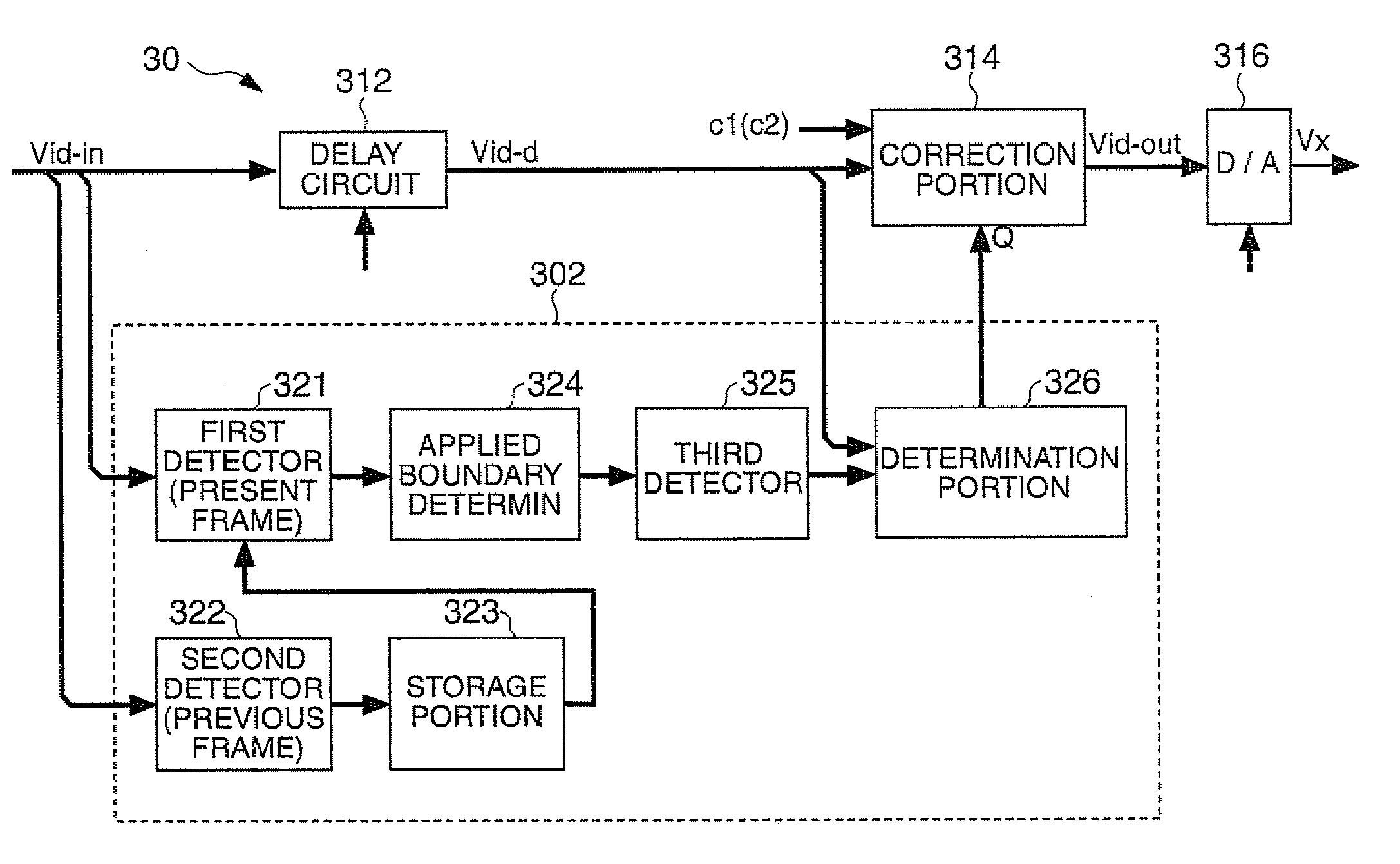
[0152]The video processing circuit 30 of this embodiment is different from that of the first embodiment, in that the content determined by the determina...

third embodiment

[0162]Next, a third embodiment of the invention will be described.

[0163]In this embodiment, instead of the dark pixel adjacent to the risk boundary, which was subjected to correction in the first embodiment, the gradation level of a bright pixel positioned on the opposite side of the risk boundary with respect to that dark pixel is corrected. However, in this embodiment, no correction is performed for the dark pixel. In this embodiment, instead of increasing the gradation level of a dark pixel in order to suppress the occurrence of a state where “(3) the liquid crystal molecules of a pixel that transitions to that bright pixel in the n-th frame are in the unstable state in the (n−1)-th frame one frame before the n-th frame,” the horizontal electric field is suppressed with attention paid to the condition “(1) when an n-th frame is focused on, a dark pixel and a bright pixel are adjacent, namely a pixel in which the applied voltage is low and a pixel in which the applied voltage is h...


PUM


Abstract

A video processing circuit used in a liquid crystal panel, includes: a first boundary detector that analyzes a video signal of a present frame to detect a boundary between a first pixel and a second pixel; a second boundary detector that analyzes a video signal of a frame one frame before the present frame to detect a boundary between the first pixel and the second pixel; a third boundary detector that detects a risk boundary that is determined by a tilt azimuth of the liquid crystal; and a correction portion that corrects an applied voltage to a liquid crystal device corresponding to a first pixel from the applied voltage to a liquid crystal device corresponding to the first pixel to a third voltage or higher, when the applied voltage specified by the video signal input to the first pixel is lower than the third voltage.

Description

BACKGROUND[0001]1. Technical Field[0002]The present invention relates to a technique of reducing display defects in a liquid crystal panel.[0003]2. Related Art[0004]A liquid crystal panel is configured such that a liquid crystal is interposed between a pair of substrates held with a predetermined gap therebetween. Specifically, the liquid crystal panel has a configuration in which pixel electrodes are arranged in a matrix form for each pixel on one substrate, a common electrode is provided on the other substrate so as to be shared by the respective pixels, and the liquid crystal is interposed between the pixel electrodes and the common electrode. When a voltage corresponding to a gradation level is applied and held between the pixel electrode and the common electrode, the alignment state of the liquid crystal is defined for each pixel, whereby transmittance or reflectance is controlled. Therefore, in the configuration above, it can be said that among the electric field acting on the...

Claims


Application Information

Patent Timeline
Patent Type & Authority Patents(United States)
IPC IPC(8): G09G3/36G09G5/00G06F3/038
CPCG09G2360/16G09G3/3648G09G2300/0876G09G2300/0447G09G2320/103
Inventor HOSAKA, HIROYUKIIISAKA, HIDEHITO
Owner SEIKO EPSON CORP
Why Eureka
Try Eureka