Semiconductor integrated circuit

Active Publication Date: 2011-08-25
SOCIONEXT INC
View PDF4 Cites 5 Cited by
  • Summary
  • Abstract
  • Description
  • Claims
  • Application Information

AI Technical Summary

Benefits of technology

[0010]According to the second embodiment, since SRAM macros are supplied with the first supply voltage and the second supply voltage both from the outside of a semiconductor integrated circuit, there is no need to provide a power supply circuit in the semiconductor integrated circuit, thus the circuit area of a semiconductor integrated circuit can be reduced.
[0011]According to the first embodi

Problems solved by technology

However, due to reduction in feature sizes of SRAMs, effect of a variation in threshold voltages (Vt) of SRAM memory cell transistors increases, thereby causing a problem in that malfunction of SRAMs occur at a voltage less than or equal to about 1

Method used


Image

  • Semiconductor integrated circuit
  • Semiconductor integrated circuit
  • Semiconductor integrated circuit

Examples


first embodiment

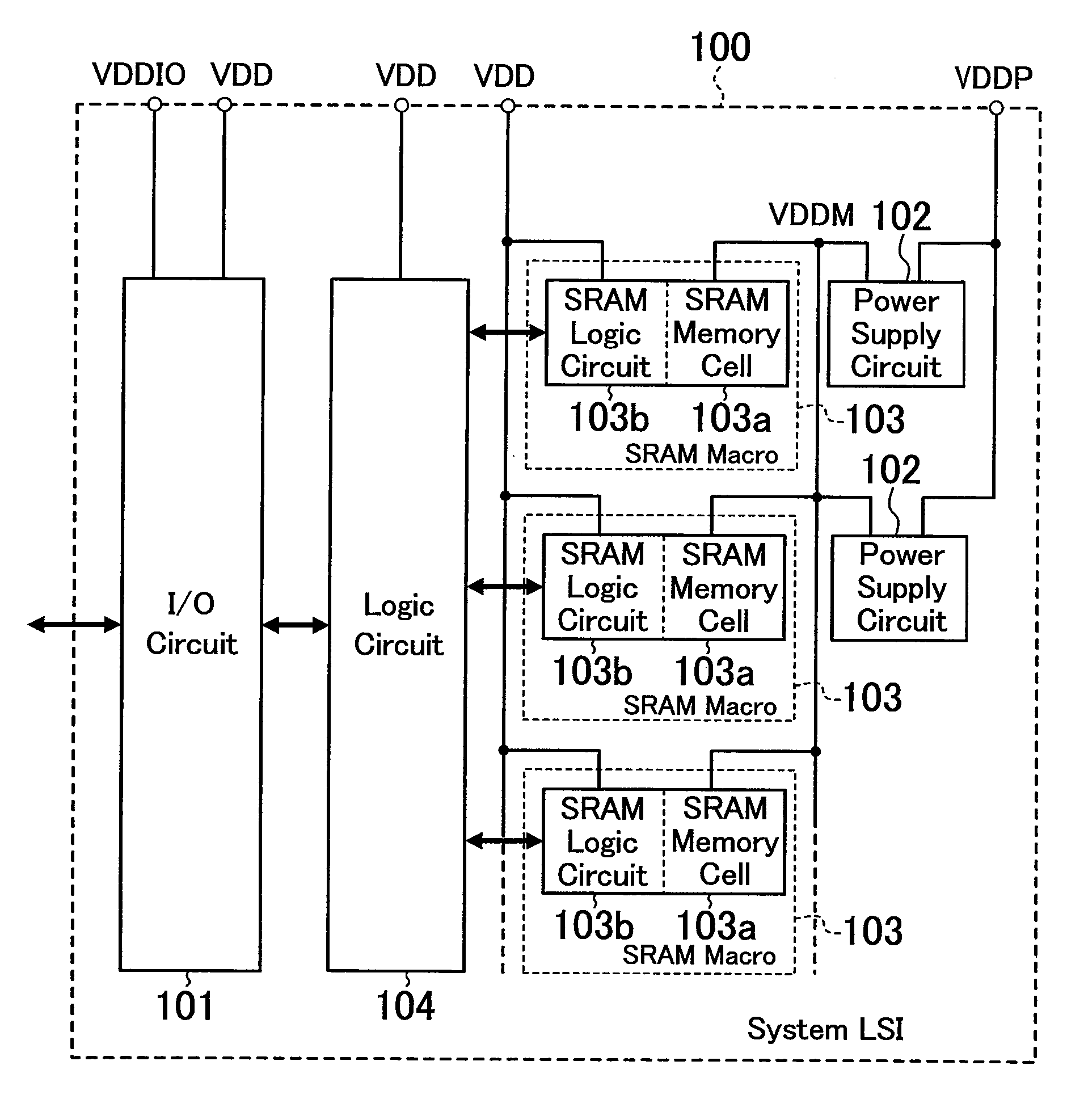
[0021]FIG. 1 illustrates a configuration of a system LSI (semiconductor integrated circuit) 100 in accordance with the first embodiment. The system LSI 100 includes an I / O circuit 101, a plurality of power supply circuits 102, a multitude of SRAM macros 103, and a logic circuit 104. The system LSI 100 is encapsulated within a package.

[0022]The I / O circuit 101 is an external interface section between the system LSI 100 and the outside thereof, and the external interface section is supplied with a voltage VDDIO (e.g., 3.3 V) and a signal voltage VDD (e.g., 1.1 V) (a second supply voltage) for use in the system LSI 100.

[0023]The power supply circuits 102 each receives a voltage VDDP (a first supply voltage) supplied from the outside of the system LSI 100, and each generates a stabilized voltage VDDM (1.2 V) (a generated voltage) lower than the voltage VDDP. The power supply circuits 102 are supplied with the voltage VDDP from a same power supply line.

[0024]The SRAM macros 103 each incl...

second embodiment

[0037]FIG. 5 illustrates a system LSI 200 in accordance with the second embodiment. In the second embodiment, the system LSI 200 is provided with, in addition to the components of the system LSI 100 of the first embodiment, a logic circuit 201 capable of high-speed operation using the stabilized voltage VDDM generated by the power supply circuit 102. In addition, the SRAM logic circuit 103b′ of an SRAM macro 103′ (a second SRAM macro) which communicates with the logic circuit 201 is supplied with the stabilized voltage VDDM generated by the power supply circuit 102, instead of the voltage VDD. Note that the number of SRAM macros 103′ whose SRAM logic circuit 103b′ is supplied with the voltage VDDM may be one or more. Since the other part of the configuration is same as that of the first embodiment, identical or equivalent component parts are indicated by like reference characters, and the explanation thereof will be omitted.

[0038]Normally, the supply voltage VDD for the logic circui...

third embodiment

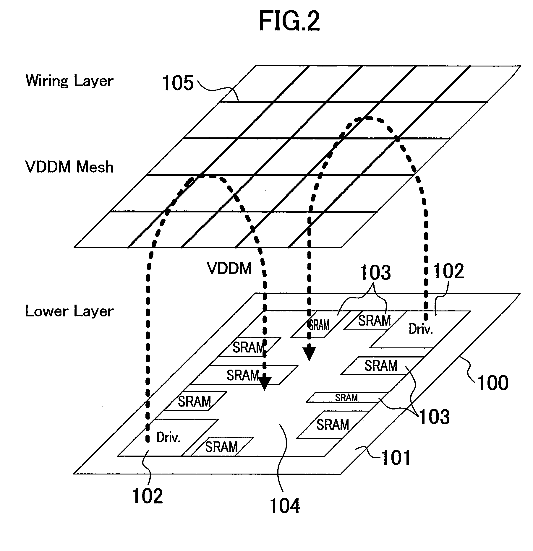
[0039]FIG. 6 illustrates a system LSI 300 in accordance with the third embodiment. In the third embodiment, lines 302 are provided on a substrate 301 formed on the system LSI 300 within a package. In addition, at a plurality of locations on the system LSI 300, area pads 303 connected to the VDDM power supply lines 105 of a mesh configuration are formed, and the area pads 303 are connected to the lines 302 through solder bumps. Moreover, the voltage VDDM generated by the power supply circuit 102 is supplied to the SRAM macros 103 through the area pads 303 and the lines 302 within the package. Since the other part of the configuration is same as that of the first embodiment, identical or equivalent component parts are indicated by like reference characters, and the explanation thereof will be omitted. Note that the features of this embodiment may be applied to the system LSI 200 of the second embodiment.

[0040]In a typical case where a sheet resistance of the lines 302 within the packa...


PUM


Abstract

A system LSI (100) having a logic circuit (104) and a plurality of SRAM macros (103) includes a power supply circuit (102) configured to receive a voltage (VDDP) supplied from the outside of the system LSI (100), and to generate a stabilized voltage (VDDM) lower than the voltage (VDDP). An SRAM memory cell (103a) of each of the plurality of SRAM macros (103) is supplied with the voltage (VDDM) generated by the power supply circuit (102), and an SRAM logic circuit (103b) of each of the plurality of SRAM macros (103) is supplied with a voltage (VDD) supplied from the outside. In addition, the logic circuit (104) is supplied with the voltage (VDD) from the outside.

Description

TECHNICAL FIELD[0001]The present disclosure relates to semiconductor integrated circuits having a plurality of SRAM (Static Random Access Memory) macros.BACKGROUND ART[0002]In recent years, with reduction in feature sizes of semiconductor processes, there has been a trend toward further increase of the number of SRAM macros embedded in a system LSI (Large Scale Integration circuit). However, due to reduction in feature sizes of SRAMs, effect of a variation in threshold voltages (Vt) of SRAM memory cell transistors increases, thereby causing a problem in that malfunction of SRAMs occur at a voltage less than or equal to about 1 V. Therefore, for system LSIs in 45-nm and 32-nm generations or later, it is suggested to use a stabilized voltage of 1.2 V as the supply voltage for SRAM memory cells, utilizing power supply circuits, thereby to ensure operating margins of SRAMs.[0003]In Non-Patent Document 1, a power supply CVDD generates a generated voltage stabilized at 1.2 V using a volta...

Claims


Application Information

Patent Timeline
IPC IPC(8): G11C5/14
CPCG11C5/147G11C11/413H01L23/5286H01L27/11H01L2924/0002H01L2924/3011H01L2924/00H10B10/00
Inventor AGATA, YASUHIRONARUMI, NORIAKIYAMAGAMI, YOSHINOBUMASUO, AKIRA
Owner SOCIONEXT INC
Why Eureka
Try Eureka