

Semiconductor device and manufacturing method thereof
a semiconductor device and semiconductor technology, applied in the field of semiconductor devices, can solve the problems of increasing s coefficient (subthreshold coefficient), limited miniaturization of devices to be formed, and reducing so as to achieve the effect of satisfying the reduction of the area of semiconductor devices and increasing the integration degree of devices
- Summary
- Abstract
- Description
- Claims
- Application Information
AI Technical Summary
Benefits of technology
Problems solved by technology
Method used
Image

Examples
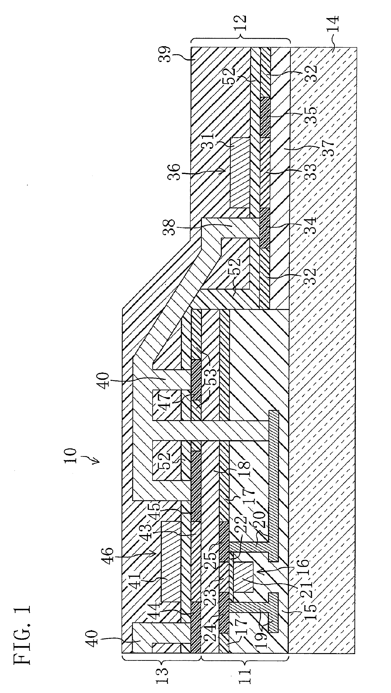
first embodiment
Advantages of First Embodiment
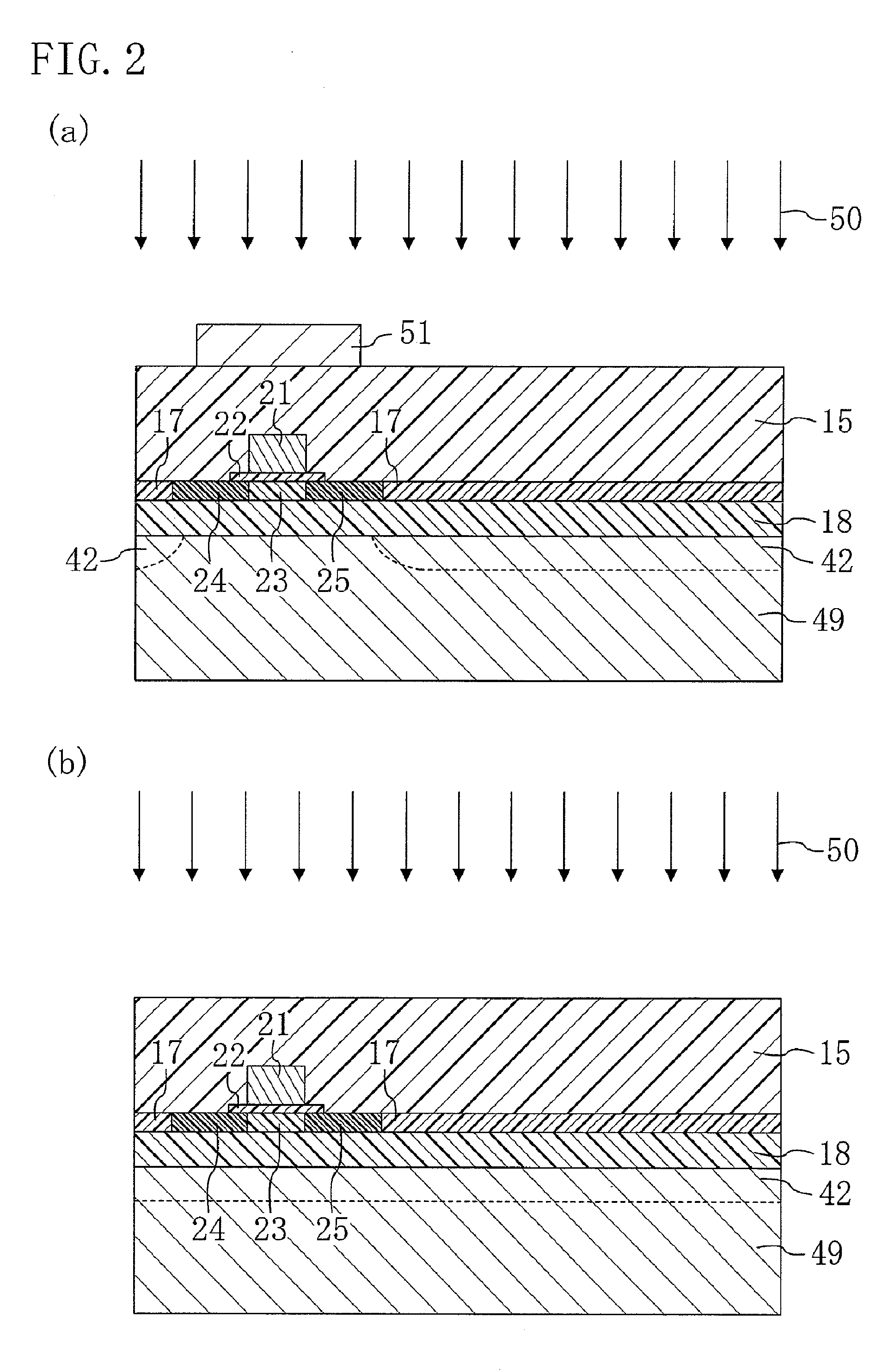
[0089]According to the first embodiment, the multilayer device part 13 is stacked on the adhered device part 11 adhered to the support substrate 14, and the adjacent device part 12 is formed in a region adjacent to the adhered device part on the support substrate 14. Moreover, the adhered device part 11, the multilayer device part 13, and the adjacent device part 12 are electrically connected to one another. Therefore, the integration degree of the devices increases. For example, a low-voltage logic circuit, a stable analog circuit, a high-voltage drive circuit, etc. can be integrated at a high degree on a given substrate such as a glass substrate, a quartz substrate, or the like larger than a silicon substrate. As a result, it is possible to satisfactorily reduce the area of the semiconductor device 10.
[0090]Moreover, the support substrate 14 has an area larger than that of the adhered device part 11. Thus, it is possible to form the adjacent device pa...
second embodiment
Advantages of Second Embodiment
[0142]According to the second embodiment, the multilayer device part 63 is stacked on the adhered device part 61 adhered to the support substrate 64, and the adjacent device part 62 is formed in a region adjacent to the adhered device part on the support substrate 64. Moreover, the adhered device part 61, the multilayer device part 63, and the adjacent device part 62 are electrically connected to one another. Therefore, the integration degree of the devices increases. For example, a low-voltage logic circuit, a stable analog circuit, a high-voltage drive circuit, etc. can be integrated at a high degree on a given substrate such as a glass substrate, a quartz substrate, or the like larger than a silicon substrate. As a result, it is possible to satisfactorily reduce the area of the semiconductor device 60.
[0143]Moreover, the support substrate 64 has an area larger than that of the adhered device part 61. Thus, it is possible to form the adjacent device ...
third embodiment
Advantages of Third Embodiment
[0151]According to the third embodiment, it is possible to provide the display device 110 having advantages such as an increase in integration degree of the devices, which satisfactorily reduces the area as in the first embodiment.
Fourth Embodiment
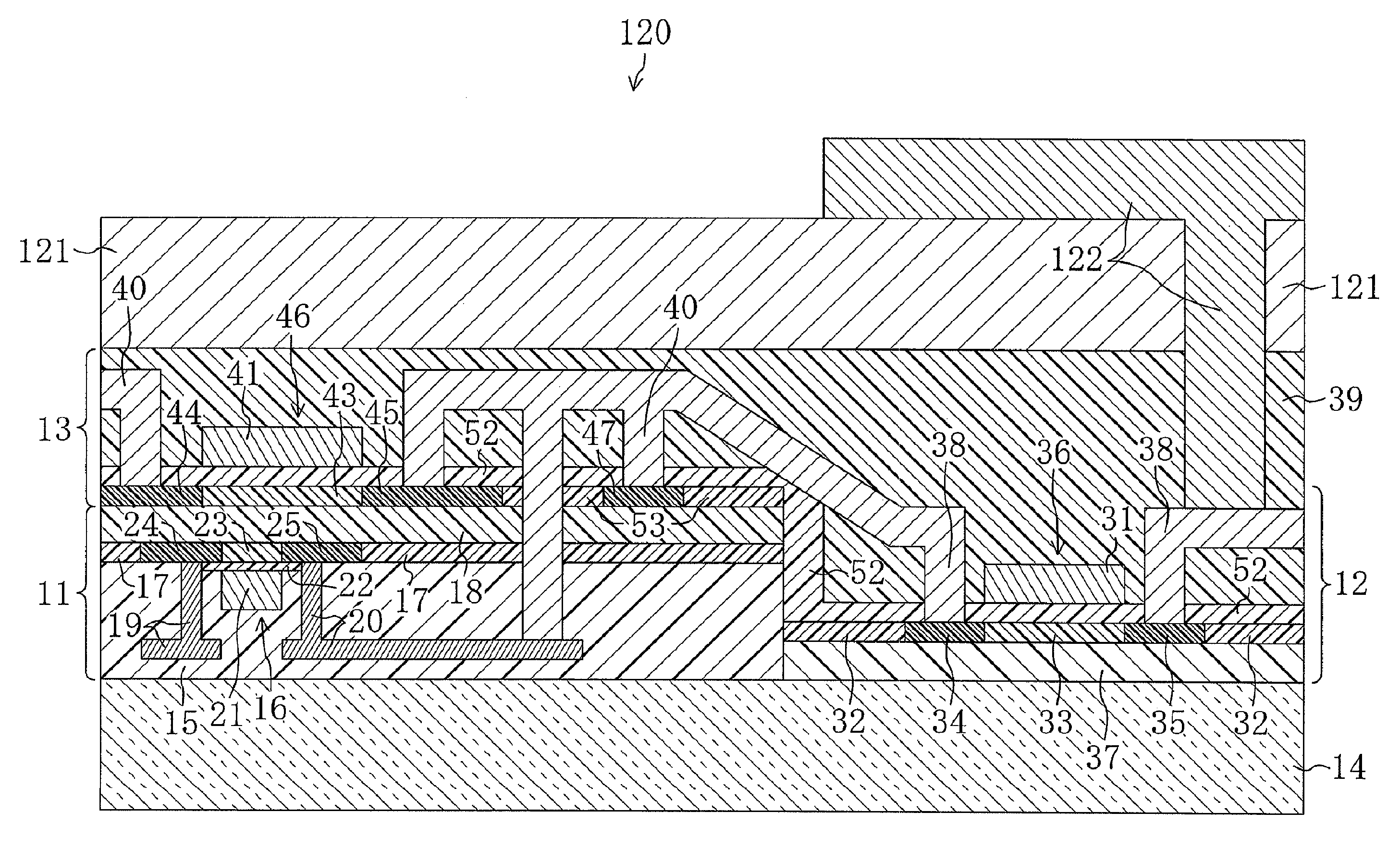
[0152]FIG. 8 is a cross-sectional view schematically illustrating main components of a display device 120 according to a fourth embodiment of the present invention. The display device 120 has a configuration in which a planarization layer 121, a display electrode 122 formed in an active matrix region, etc. are provided on the semiconductor device 10 illustrated in the first embodiment. Here, the semiconductor device used in the display device 120 is provided with a metal interconnect 38 electrically connected to the drain region 35 of the adjacent device part 12 in the semiconductor device 10 illustrated in the first embodiment.
[0153]The display electrode is electrically connected to the metal interconnect 38 ...
PUM
 Abstract
Description
Claims
Application Information