Semiconductor device

a semiconductor device and layout technology, applied in semiconductor devices, semiconductor/solid-state device details, electrical equipment, etc., can solve the problems of increasing the wiring delay of other wirings, increasing increasing power consumption, so as to improve the wiring efficiency of signal wirings, the effect of suppressing the voltage drop of the power supply wiring

Active Publication Date: 2009-07-09
PANASONIC CORP
View PDF3 Cites 3 Cited by
  • Summary
  • Abstract
  • Description
  • Claims
  • Application Information

AI Technical Summary

Benefits of technology

[0014]The present invention has been achieved to solve the problems described above. An object of the present invention is to provide a layout configuration of a semiconductor device in which a substrate control can be performed without reducing the wiring efficiency of a signal wiring, and a voltage drop of a power supply wiring can be suppressed.
[0015]To achieve the object, according to the present invention, a power supply connection portion is provided in a boundary portion of a cell, thereby improving the wiring efficiency of a signal wiring. Further, by setting the width of a power supply wiring in the cell to be larger than or equal to the width of a power supply wiring in other logic cells, a voltage drop is suppressed, thereby preventing an erroneous operation of a semiconductor device. A substrate potential is supplied via an upper-layer power supply wiring to the power supply connection portion, thereby changing a substrate potential so that a leakage current can be reduced.
[0016]The semiconductor device of the present invention has a layout configuration in which standard cells are arranged side by side, and a potential different from a power supply voltage can be supplied to a well substrate, so that a leakage current can be reduced and therefore, the power consumption of the semiconductor device can be reduced.
[0017]Also, the potential can be supplied to the well substrate without reducing signal wiring efficiency, resulting in a reduction in area of the semiconductor device. Also, the semiconductor device of the present invention has a power supply wiring configuration that can suppress a voltage drop, thereby making it possible to prevent an erroneous operation of the semiconductor device.

Problems solved by technology

In recent years, as a semiconductor device has been further miniaturized, an increase in power consumption has become more significant due to an increase in leakage current.
In either case, a wiring resistance increases and therefore a wiring delay increases.
In addition, the wiring detour deteriorates wiring efficiency in the vicinity of the substrate power supply cell 1300, leading to an increase in wiring delay of other wirings.
If the substrate power supply wiring 1320 has a high resistance, and therefore, the substrate power supply cells 1300 should be spaced from each other by a short distance, the wiring detour frequently occurs, so that the timing design of the semiconductor device is adversely affected.
As the number of portions in which the power supply wiring 1520 has a narrow width increases, the wiring resistance of the power supply wiring 1520 increases, so that a voltage drop is more likely to occur during an operation of the semiconductor device, leading to an erroneous operation of the semiconductor device.

Method used


Image

  • Semiconductor device
  • Semiconductor device
  • Semiconductor device

Examples


first embodiment

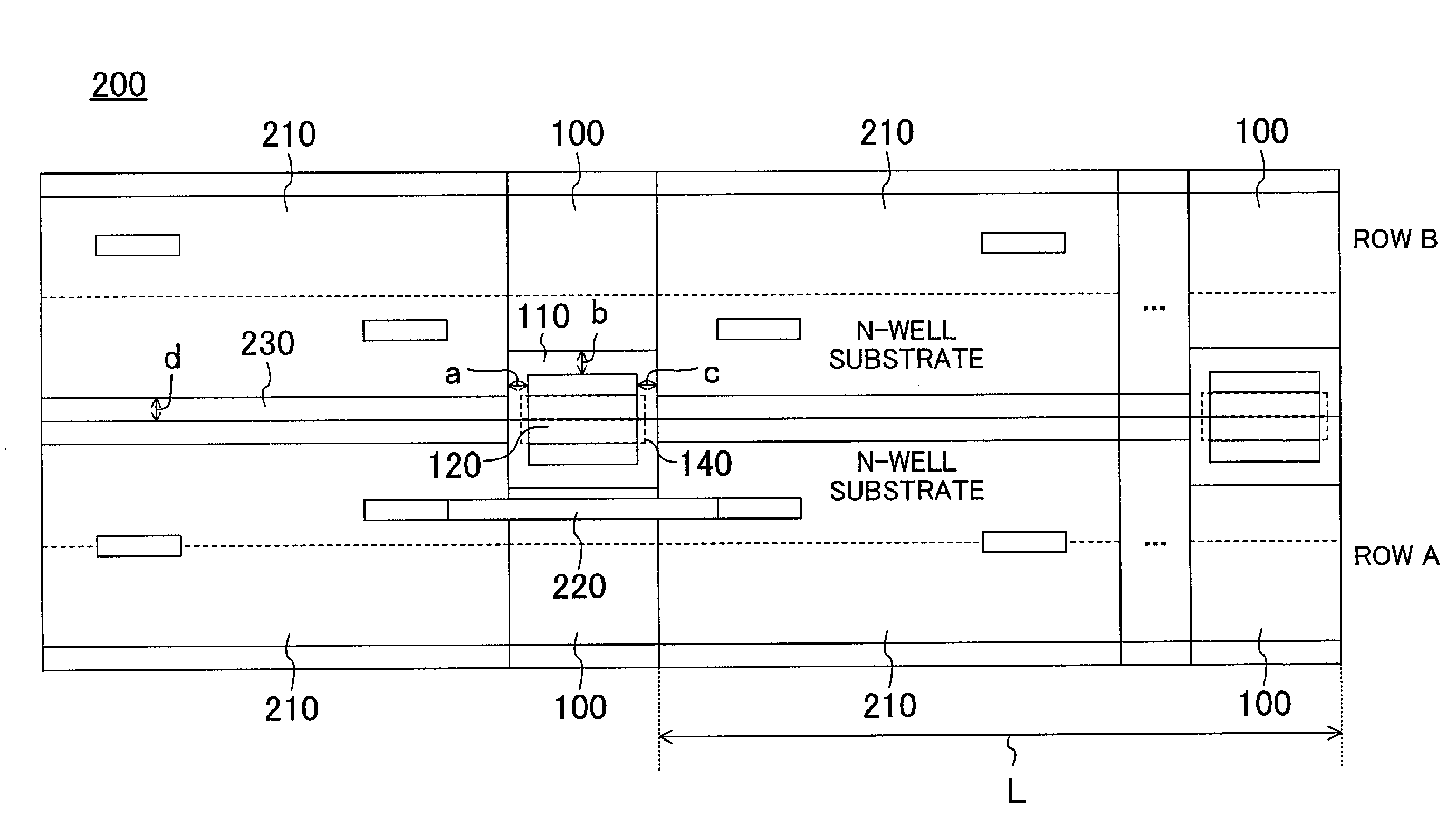
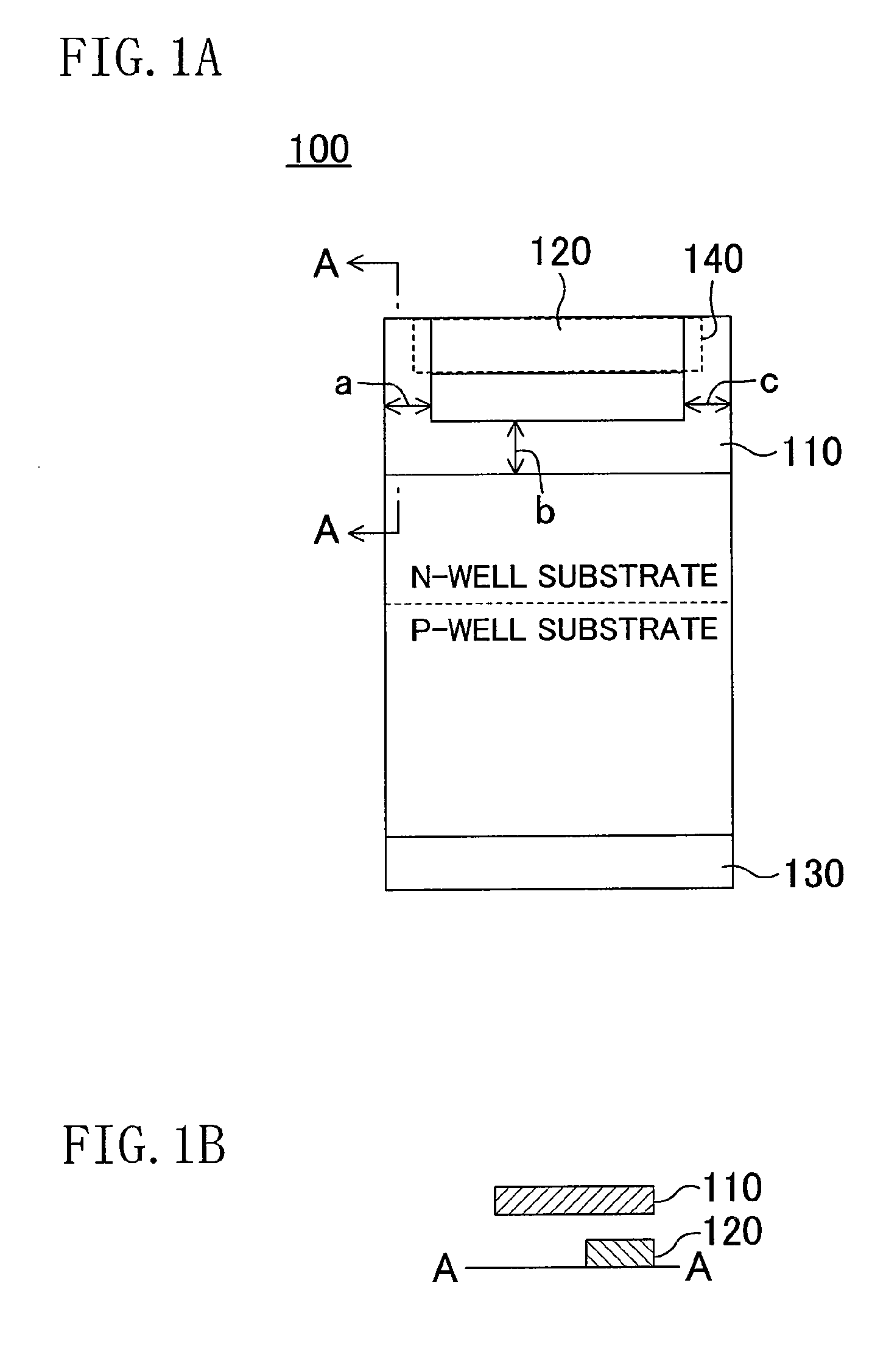
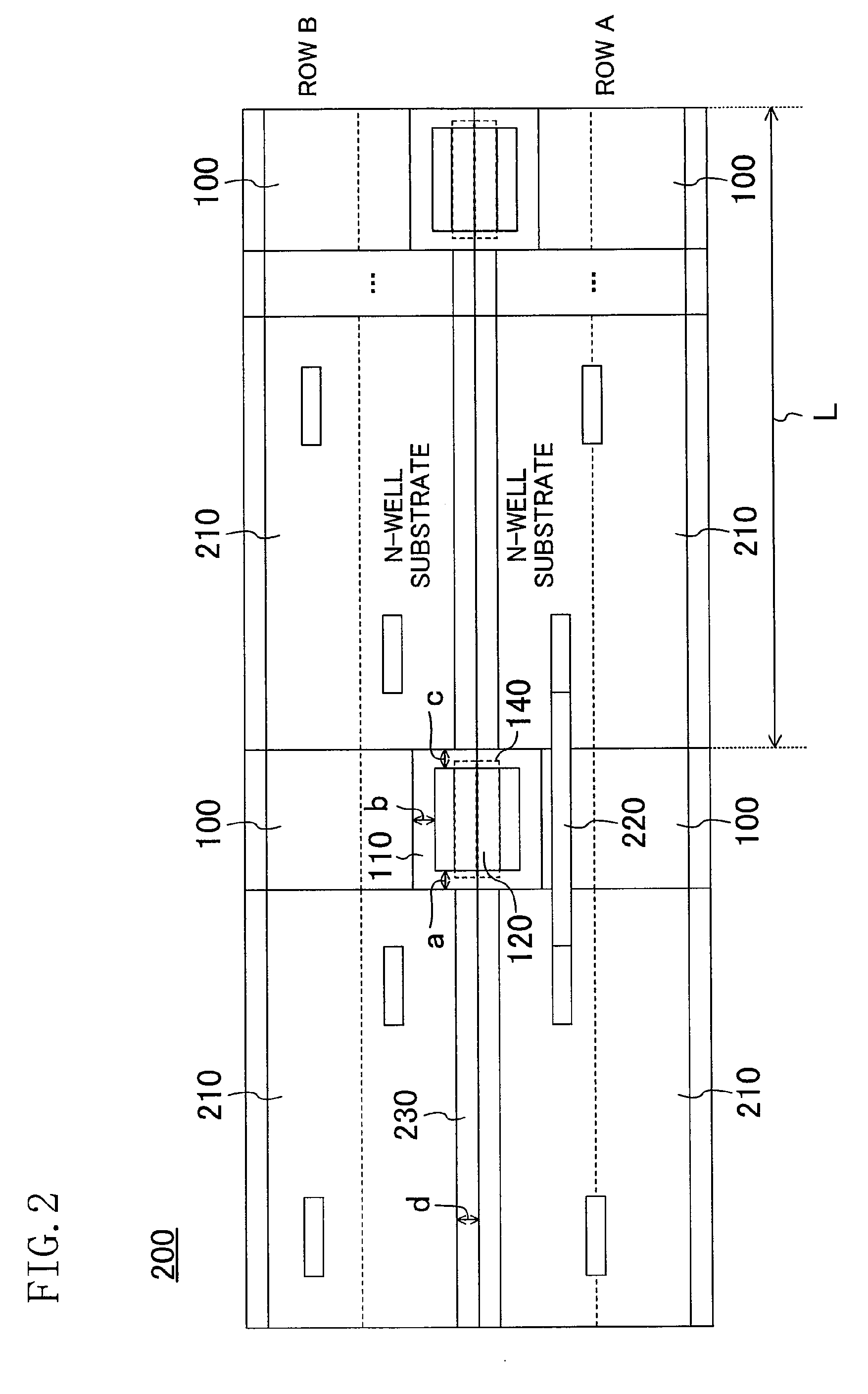
[0041]FIG. 1A shows a layout configuration of a substrate power supply cell 100 according to a first embodiment of the present invention. In FIG. 1A, the substrate power supply cell 100 is divided at a middle thereof into an N-well substrate region and a P-well substrate region. The substrate power supply cell 100 also has a power supply wiring 110, a substrate power supply wiring 120, and a ground wiring 130. The power supply wiring 110 is formed of a lowermost wiring layer, and the substrate power supply wiring 120 is formed of an impurity diffusion layer.

[0042]FIG. 1B shows a cross-sectional view taken along A-A of FIG. 1A. The power supply wiring 110 and the substrate power supply wiring 120 are not electrically connected in the substrate power supply cell 100. The substrate power supply wiring 120 is connected via a contact to an upper-layer wiring at a substrate power supply connection portion 140 that is a portion of the substrate power supply wiring 120. Widths a, b and c of...

second embodiment

[0052]FIG. 9A shows a layout configuration of a first-type substrate power supply cell 900 according to a second embodiment of the present invention, and FIG. 9B shows a layout configuration of a second-type substrate power supply cell 950 according to the second embodiment. In FIGS. 9A and 9B, the substrate power supply cells 900 and 950 are each divided into an N-well substrate region and a P-well substrate region in a middle thereof.

[0053]In FIG. 9A, the first-type substrate power supply cell 900 has a power supply wiring 910, a substrate power supply wiring 920, and a ground wiring 930. The power supply wiring 910 is formed of a lowermost wiring layer, and the substrate power supply wiring 920 is formed of an impurity diffusion layer.

[0054]FIG. 9C shows a cross-sectional view taken along line C-C of FIG. 9A. The power supply wiring 910 and the substrate power supply wiring 920 are not electrically connected. The substrate power supply wiring 920 is connected to an upper-layer wi...


PUM


Abstract

In a substrate power supply cell, a portion of a substrate power supply wiring is exposed by forming a power supply wiring in a U-shape, and a connection portion to an upper-layer wiring is provided at a boundary portion of the substrate power supply cell. Thereby, a leakage current is reduced without a decrease in signal wiring efficiency.

Description

BACKGROUND OF THE INVENTION[0001]1. Field of the Invention[0002]The present invention relates to a layout configuration of a semiconductor device, and more particularly, to a configuration of wirings and contacts for providing substrate power supply or normal power supply to a semiconductor device.[0003]2. Description of the Related Art[0004]In recent years, as a semiconductor device has been further miniaturized, an increase in power consumption has become more significant due to an increase in leakage current. Therefore, in order to suppress the increase of the leakage current, the well substrate potential of a semiconductor device is changed to a value that is different from a power supply voltage so that a threshold voltage with respect to the power supply voltage is increased, thereby reducing the leakage current. This is a well-known technique.[0005]Here, a configuration for supplying a potential different from a power supply voltage to a well substrate in a layout configurati...

Claims


Application Information

Patent Timeline
Patent Type & Authority Applications(United States)
IPC IPC(8): H01L27/10
CPCH01L27/0207H01L27/11898H01L2924/0002H01L2924/00
Inventor KISHISHITA, KEISUKE
Owner PANASONIC CORP
Why Eureka
Try Eureka