Spatial Correlation-Based Estimation of Yield of Integrated Circuits

a technology of integrated circuits and spatial correlation, applied in the field of integrated circuit design, can solve problems such as inability to physically implement design changes and then ascertain, design changes can conflict, and electrical shortening yields can be degraded

Active Publication Date: 2011-09-08
TAIWAN SEMICON MFG CO LTD
View PDF3 Cites 9 Cited by
  • Summary
  • Abstract
  • Description
  • Claims
  • Application Information

AI Technical Summary

Problems solved by technology

However, even when these rules are followed, some design changes can conflict.
For example, adding redundant wiring vias improves the yield with regard to electrical opens, but can degrade the yield with regard to electrical shorts as a result of the expanded metal shapes associated with the additional vias.
In most instances, it is impractical (if at all possible) to physically implement design changes and then ascertain how those changes impact the yield, especially given the costs associated with manufacturing today's high-density circuits.
It would be impractical, both from a time and budgetary standpoint, to ‘mock up’ different designs in hopes of determining which design provides the best yield.
With VLSI, however, the sheer number of elements present prevents conventional yield estimation techniques from operating in a time-effective manner.
Thus, manufacturing capabilities become severely limited by the design process.

Method used


Image

  • Spatial Correlation-Based Estimation of Yield of Integrated Circuits
  • Spatial Correlation-Based Estimation of Yield of Integrated Circuits
  • Spatial Correlation-Based Estimation of Yield of Integrated Circuits

Examples


Embodiment Construction

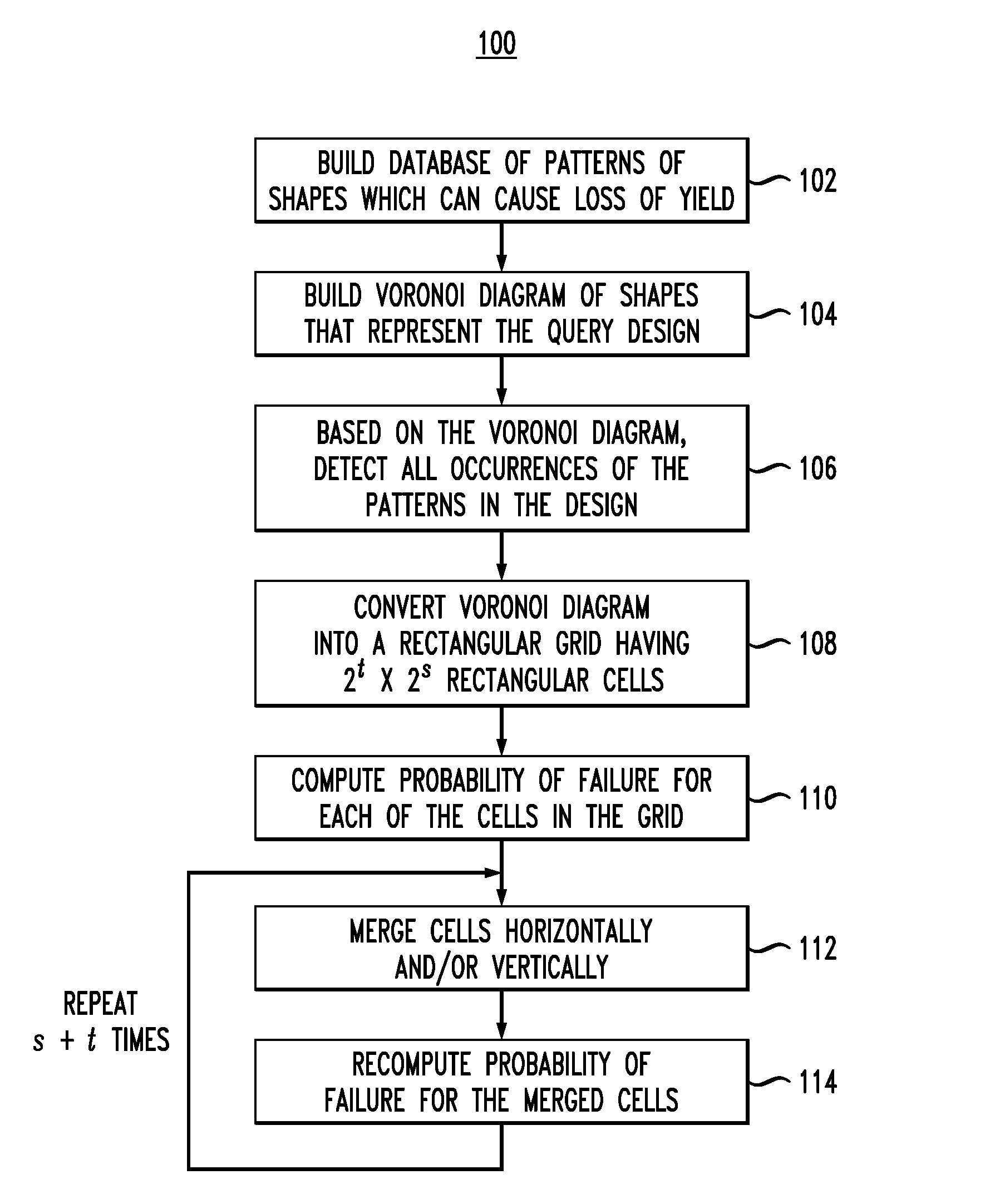
[0025]FIG. 1 is a diagram illustrating exemplary methodology 100 for determining a probability of failure of a very-large-scale integration (VLSI) query design. The present techniques provide VLSI design engineers with a tool to trace causes of yield loss in a design. Importantly, the present techniques can be performed fast enough to allow adjustments to be made to the design in a real-time interactive mode.

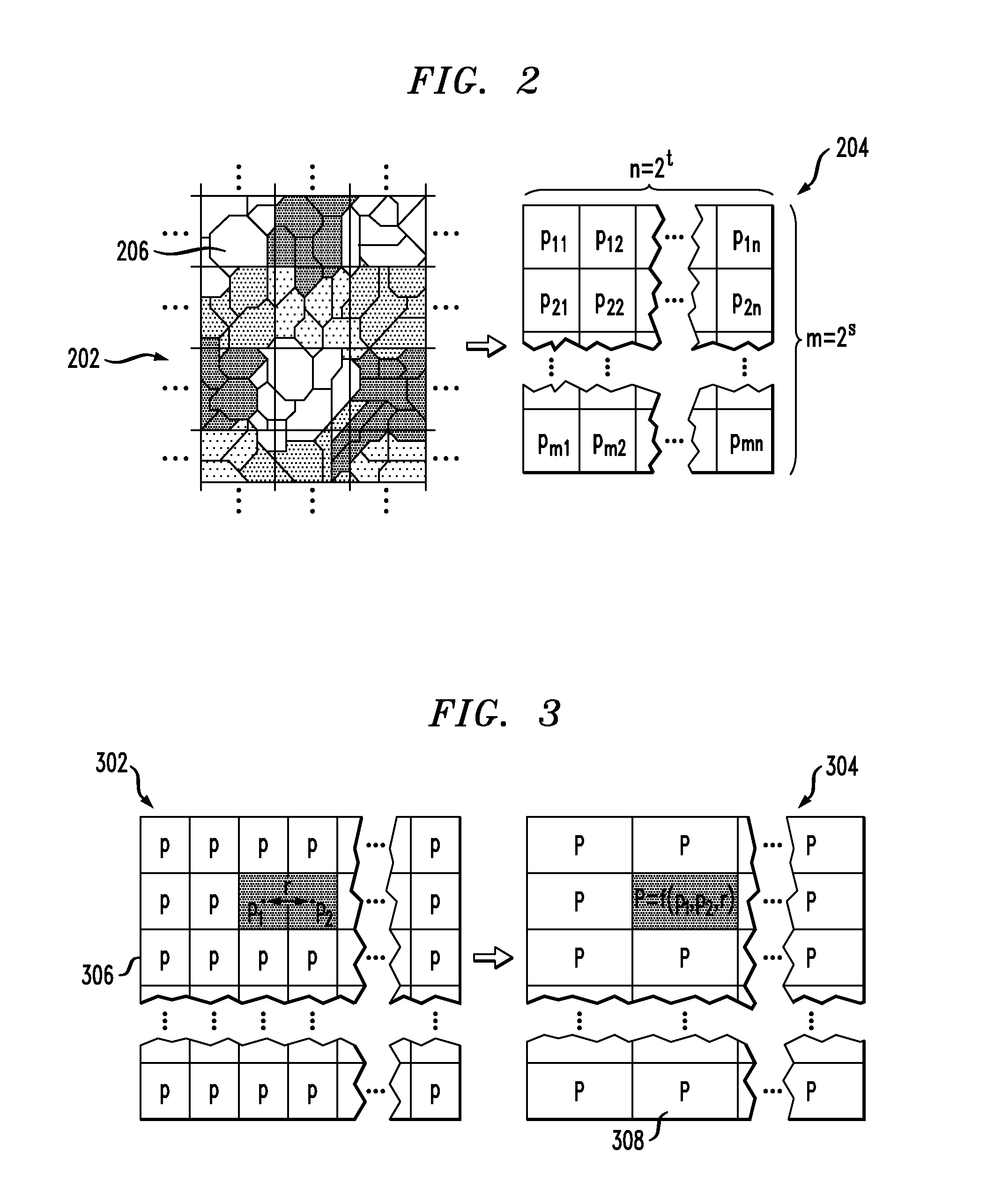
[0026]In step 102, a database is built of patterns of shapes which can potentially cause a loss of yield of a design. The most likely candidates are the patterns which break some recommended design rules and are only a couple of nanometers (nm) away from breaking some design ground rule. For example, a typical ground rule is that two wires cannot be closer than 90 nm to each other. Therefore, if two wires in a given pattern are 92 nm away from each other, then that pattern is only two nm away from breaking the ground rule. This database has to be built only once for a given tech...


PUM


Abstract

Techniques for estimating yield of an integrated circuit design, such as a very-large-scale integration (VLSI) design, are provided. In one aspect, a method for determining a probability of failure of a VLSI query design includes the following steps. A Voronoi diagram is built comprising a set of shapes that represent the design. The Voronoi diagram is converted into a rectangular grid comprising 2t×2s rectangular cells, wherein t and s are chosen so that one rectangular cell contains from about one to about five Voronoi cells. A probability of failure is computed for each of the cells in the grid. The cells in the grid are merged pairwise. A probability of failure for the merged cells is recomputed which accounts for a spatial correlation between the cells. The pairwise merge and recompute steps are performed s+t times to determine the probability of failure of the design.

Description

FIELD OF THE INVENTION[0001]The present invention relates to integrated circuit design, and more particularly, to techniques for estimating yield of an integrated circuit design.BACKGROUND OF THE INVENTION[0002]Integrated circuit design requires adherence to a basic set of design ground rules. Additional recommended rules may apply when one wants to make design changes to improve production yield of a particular design. However, even when these rules are followed, some design changes can conflict. For example, adding redundant wiring vias improves the yield with regard to electrical opens, but can degrade the yield with regard to electrical shorts as a result of the expanded metal shapes associated with the additional vias.[0003]Thus, determining the effects certain design changes will have on yield is an important factor in integrated circuit development. In most instances, it is impractical (if at all possible) to physically implement design changes and then ascertain how those ch...

Claims


Application Information

Patent Timeline
Patent Type & Authority Applications(United States)
IPC IPC(8): G06F17/50
CPCG06F17/50G06F30/00G06F2111/08G06F30/398
Inventor HENG, FOOK-LUENLVOV, ALEXEY Y.SINGHEE, AMITH
Owner TAIWAN SEMICON MFG CO LTD
Why Eureka
Try Eureka