Ground structures in resonators for planar and folded distributed electromagnetic wave filters

a distributed electromagnetic wave filter and ground structure technology, applied in waveguides, basic electric elements, waveguide type devices, etc., to achieve the effect of reducing interference with current, narrowing the effective cavity width, and increasing the attenuation of wave propagation

Active Publication Date: 2011-09-22
RAYTHEON CO
View PDF14 Cites 25 Cited by
  • Summary
  • Abstract
  • Description
  • Claims
  • Application Information

AI Technical Summary

Benefits of technology

[0015]This is accomplished by forming one or more holes in one or more of the resonators (planar or folded) and by passing a conductive structure through each hole normal to the resonator. The conductive structures (vertical vias or horizontal strips) are preferably grounded, either by direct connection or capacitive coupling to one or more ground planes or by creation of a virtual ground. The holes are spaced apart from the edges of the resonator so as to minimize any interference with the current and fields concentrated at the edges of each resonator. These conductive structures narrow the effective cavity width “aeff” for the waveguide as a whole and between non-adjacent resonators without affecting the cavity width “a” between adjacent resonators. Consequently the conductive structures have no effect on the desired coupling between adjacent resonators and the desired filter response of parallel-coupled filters while increasing the attenuation of the wave propagating in the waveguide and the attenuation of the wave coupled between non-adjacent resonators. In a direct-coupled filter topology, additional conductive structures may be placed between the resonators to effectively reduce the between resonator cavity width as well so that the filter response is determined by the directly coupled wave.

Problems solved by technology

Consequently the conductive structures have no effect on the desired coupling between adjacent resonators and the desired filter response of parallel-coupled filters while increasing the attenuation of the wave propagating in the waveguide and the attenuation of the wave coupled between non-adjacent resonators.

Method used


Image

  • Ground structures in resonators for planar and folded distributed electromagnetic wave filters
  • Ground structures in resonators for planar and folded distributed electromagnetic wave filters
  • Ground structures in resonators for planar and folded distributed electromagnetic wave filters

Examples


Embodiment Construction

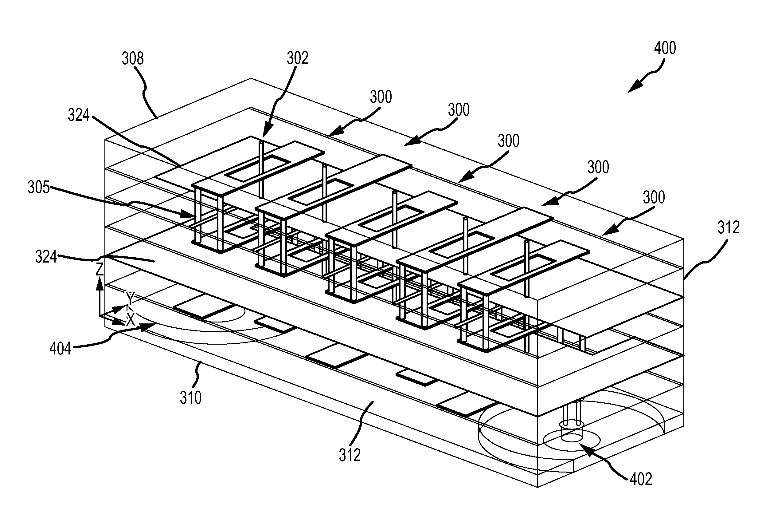
[0029]The present invention describes distributed electromagnetic wave filters with reduced coupling between non-adjacent resonators and reduced wave propagation through the waveguide structure. This is accomplished by forming one or more holes in one or more of the resonators (planar or folded) and by passing a conductive structure through each hole normal to the resonator. The conductive structures (vertical vias or horizontal strips) are preferably grounded, either by connection to one or more ground planes, capacitive coupling to a ground plane or by creation of a virtual ground. The holes are spaced apart from the edges of the resonator so as to minimize any interference with the current and fields concentrated at the edges of each resonator. These conductive structures narrow the effective cavity width “aeff” for the waveguide as a whole and between non-adjacent resonators without affecting the cavity width “a” between adjacent resonators. Consequently the conductive structure...


PUM


Abstract

Coupling between non-adjacent resonators and wave propagation through the waveguide structure in distributed EM filters are reduced by forming one or more holes in one or more of the resonators (planar or folded) and by passing a conductive structure through each hole normal to the resonator. The conductive structures (vertical vias or horizontal strips) are preferably grounded, either by direct connection or capacitive coupling to one or more ground planes or by creation of a virtual ground. The holes are spaced apart from the edges of the resonator so as to minimize any interference with the current and fields concentrated at the edges of each resonator. These conductive structures narrow the effective cavity width “aeff” for the waveguide as a whole and between non-adjacent resonators without affecting the cavity width “a” between adjacent resonators. Consequently the conductive structures have no effect on the desired coupling between adjacent resonators and the desired filter response of parallel-coupled filters while increasing the attenuation of the wave propagating in the waveguide and the attenuation of the wave coupled between non-adjacent resonators.

Description

BACKGROUND OF THE INVENTION[0001]1. Field of the Invention[0002]This invention relates to distributed electromagnetic wave filters and more particularly to ground structures formed in the resonators for planar and folded filters.[0003]2. Description of the Related Art[0004]A distributed element filter is an electromagnetic (EM) wave filter designed for frequencies between approximately 100 MHz to approximately 100 GHz and more typically between 500 MHz and 60 GHz. These bands may be referred to as RF or microwave. At these frequencies, the physical length of passive components is a significant fraction of the wavelength of the operating frequency, and it becomes difficult to use the conventional lumped element model. The distributed element model allows these components to be designed using transmission line theory better suited for these frequencies. These filters may be configured as lowpass, highpass, band pass or bandstop filters.[0005]The filter is made up of one or more couple...

Claims


Application Information

Patent Timeline
Patent Type & Authority Applications(United States)
IPC IPC(8): H01P1/205
CPCH01P1/20336H01P1/2039H01P1/20345
Inventor PATRICK, KEVIN W.BALDWIN, JEREMY B.BLUMKE, JOEL C.CARDONA, SERGIO E.KARASIEWICZ, DAVID J.
Owner RAYTHEON CO
Why Eureka
Try Eureka