Methods of Forming Semiconductor Devices Having Faceted Semiconductor Patterns

a technology of semiconductor devices and patterns, applied in the direction of semiconductor devices, electrical equipment, transistors, etc., can solve the problems that the semiconductor (pmos) transistor may face several obstacles, and achieve excellent electrical characteristics

Active Publication Date: 2011-09-22
SAMSUNG ELECTRONICS CO LTD
View PDF8 Cites 39 Cited by
  • Summary
  • Abstract
  • Description
  • Claims
  • Application Information

AI Technical Summary

Problems solved by technology

Although research has been conducted regarding various ways to improve electrical characteristics of transistors, fabrication of p-channel metal-oxide-semiconductor (PMOS) transistors may face several obstacles with regard to controlling locations of source and drain regions and lightly doped drain (LDD) regions.

Method used


Image

  • Methods of Forming Semiconductor Devices Having Faceted Semiconductor Patterns
  • Methods of Forming Semiconductor Devices Having Faceted Semiconductor Patterns
  • Methods of Forming Semiconductor Devices Having Faceted Semiconductor Patterns

Examples


Embodiment Construction

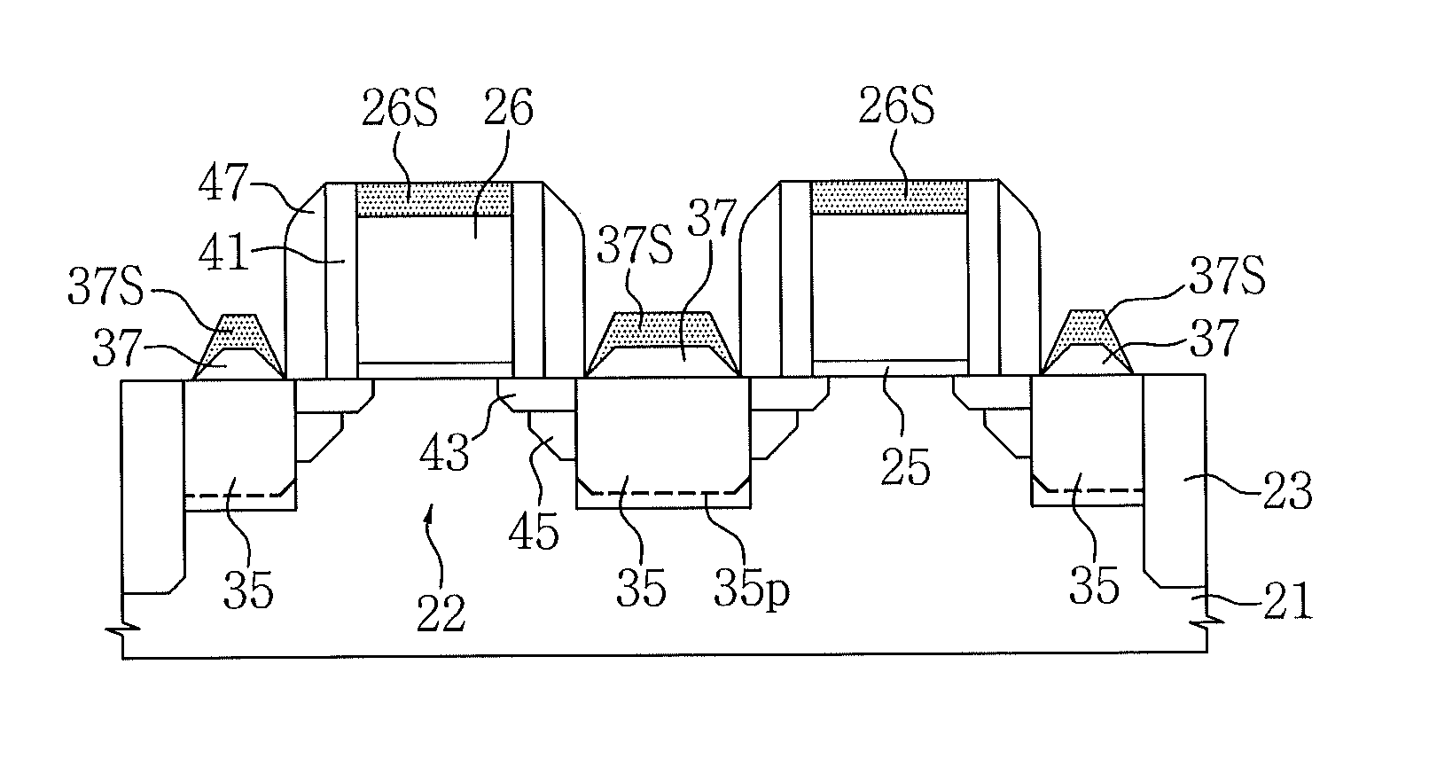
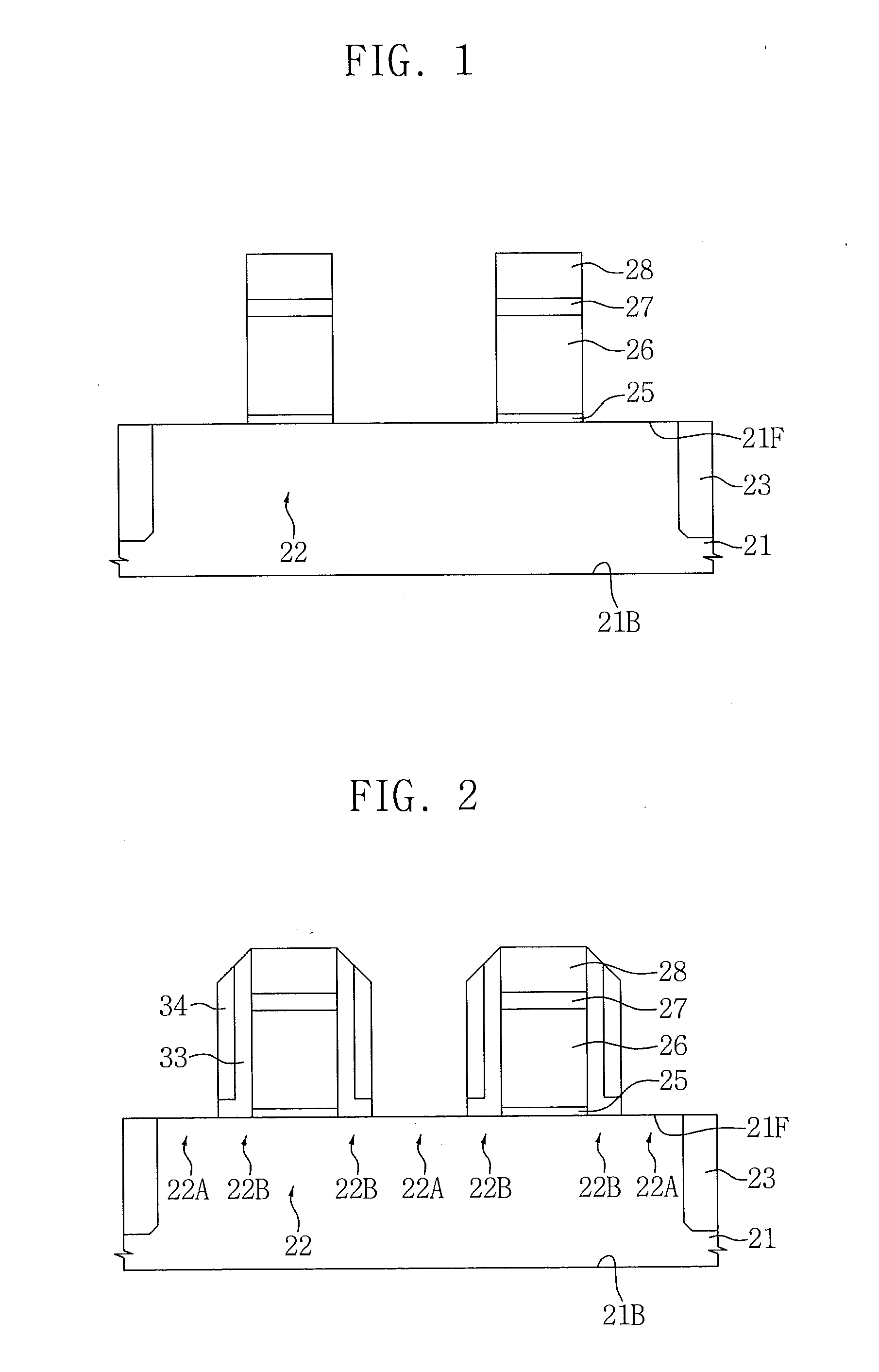
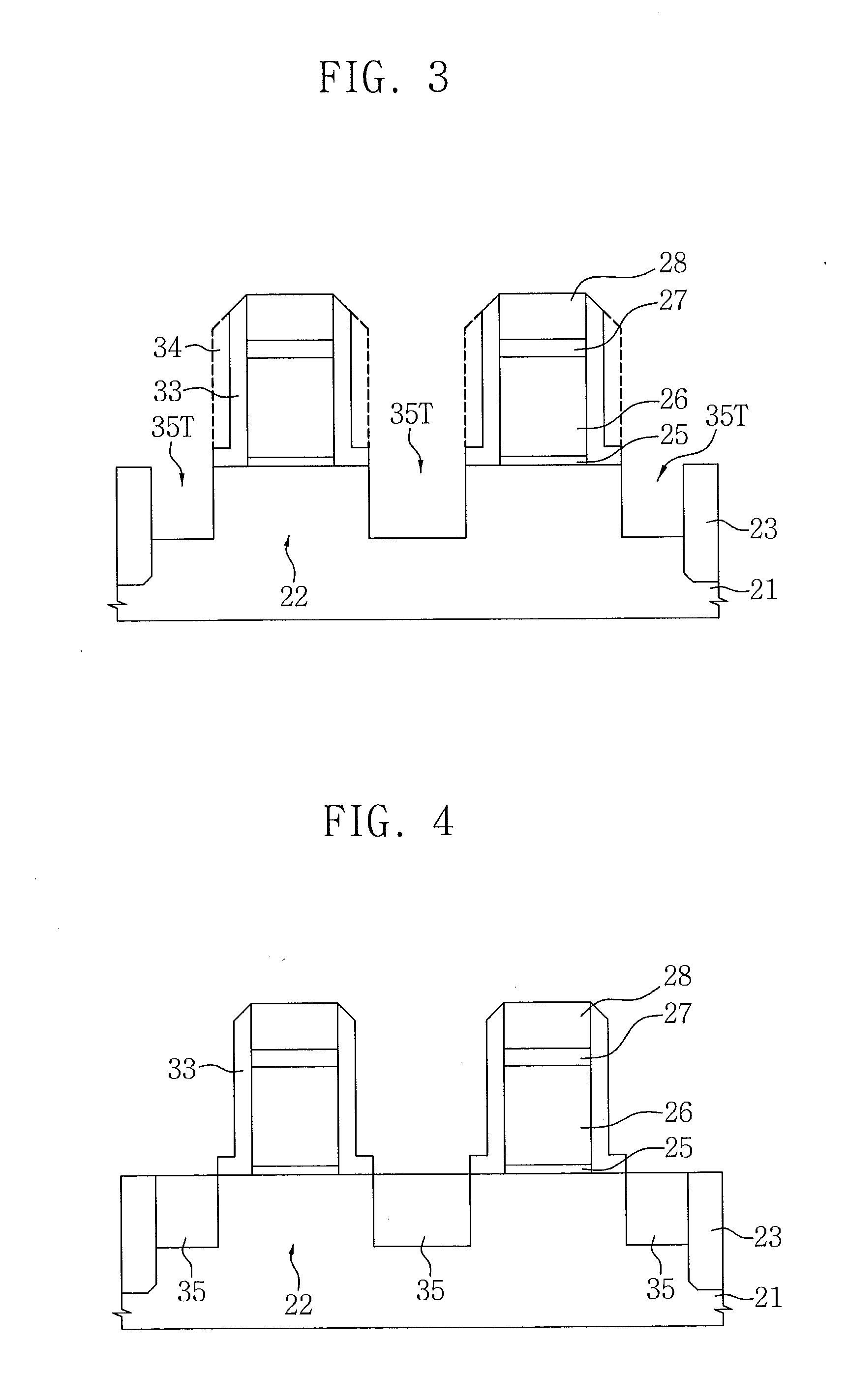
[0035]Example embodiments will be described below in more detail with reference to the accompanying drawings. Many different forms and embodiments are possible without deviating from the spirit and teachings of this disclosure and so the disclosure should not be construed as limited to the embodiments set forth herein. Rather, these embodiments are provided so that this disclosure will be thorough and complete, and will fully convey the scope of the disclosure to those skilled in the art. In the drawings, the sizes and relative sizes of layers and regions may be exaggerated for clarity. Like reference numbers refer to like elements throughout.

[0036]The terminology used herein is for the purpose of describing particular embodiments only and is not intended to be limiting of the embodiments. As used herein, the singular forms “a”, “an,” and “the” are intended to include the plural forms as well, unless the context clearly indicates otherwise. It will be further understood that the ter...


PUM


Abstract

Provided are methods of forming semiconductor devices. A method may include preparing a semiconductor substrate including a first region and a second region adjacent the first region. The method may also include forming sacrificial pattern covering the second region and exposing the first region. The method may further include forming a capping layer including a faceted sidewall on the first region using selective epitaxial growth (SEG). The faceted sidewall may be separate from the sacrificial pattern. The sacrificial pattern may be removed. Impurity ions may be implanted into the semiconductor substrate.

Description

CROSS-REFERENCE TO RELATED APPLICATION[0001]This U.S. non-provisional patent application claims priority under 35 U.S.C. §119 to Korean Patent Application No. 10-2010-0024789, filed on Mar. 19, 2010, the disclosure of which is hereby incorporated by reference in its entirety.BACKGROUND[0002]1. Field[0003]The present disclosure herein relates to methods of forming semiconductor devices, and more particularly, to methods of forming semiconductor devices having faceted semiconductor patterns.[0004]2. Description of Related Art[0005]Although research has been conducted regarding various ways to improve electrical characteristics of transistors, fabrication of p-channel metal-oxide-semiconductor (PMOS) transistors may face several obstacles with regard to controlling locations of source and drain regions and lightly doped drain (LDD) regions.SUMMARY[0006]The present disclosure provides methods of forming semiconductor devices having excellent electrical characteristics.[0007]Some embodim...

Claims


Application Information

Patent Timeline
Patent Type & Authority Applications(United States)
IPC IPC(8): H01L21/336
CPCH01L21/26586H01L29/165H01L29/665H01L29/7834H01L29/6659H01L29/66628H01L29/66636H01L29/6653H01L21/02293
Inventor KIM, MYUNG-SUNSHIN, DONG-SUKKIM, DONG-HYUKLEE, YONG-JOOCHUNG, HOI-SUNG
Owner SAMSUNG ELECTRONICS CO LTD
Why Eureka
Try Eureka