

Low side zener reference voltage extended drain SCR clamps
a technology of reference voltage and scr clamps, applied in the direction of semiconductor devices, semiconductor/solid-state device details, electrical apparatus, etc., can solve the problem of unpredictability of triggering under different loads
- Summary
- Abstract
- Description
- Claims
- Application Information
AI Technical Summary
Benefits of technology
Problems solved by technology
Method used
Image

Examples
Embodiment Construction
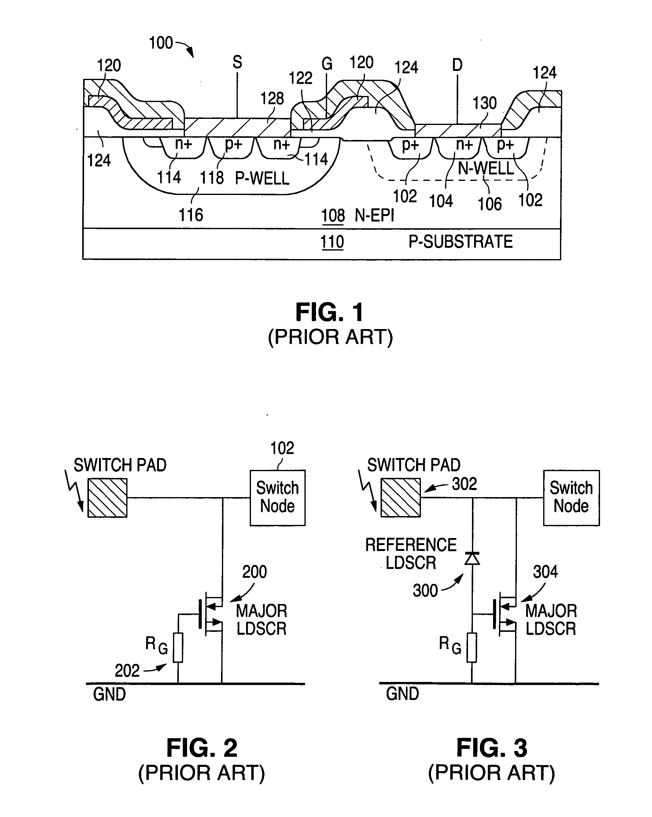
[0015]A typical LDMOS-SCR as known in the art was described above with respect to FIG. 1 with its n+ drain 104 formed in an n-well 106 and n+ source regions 118 formed in a p-well 116. The n-well defines a short drift region extending to underneath the gate poly 120. The device is bounded on either side by an isolation region (not shown).
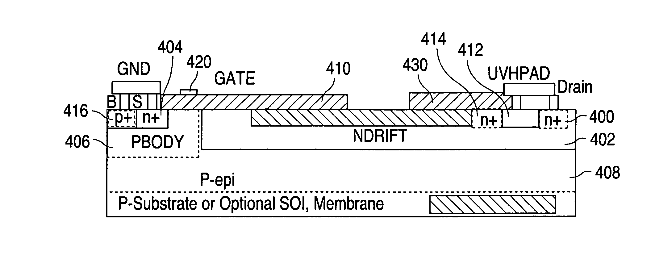
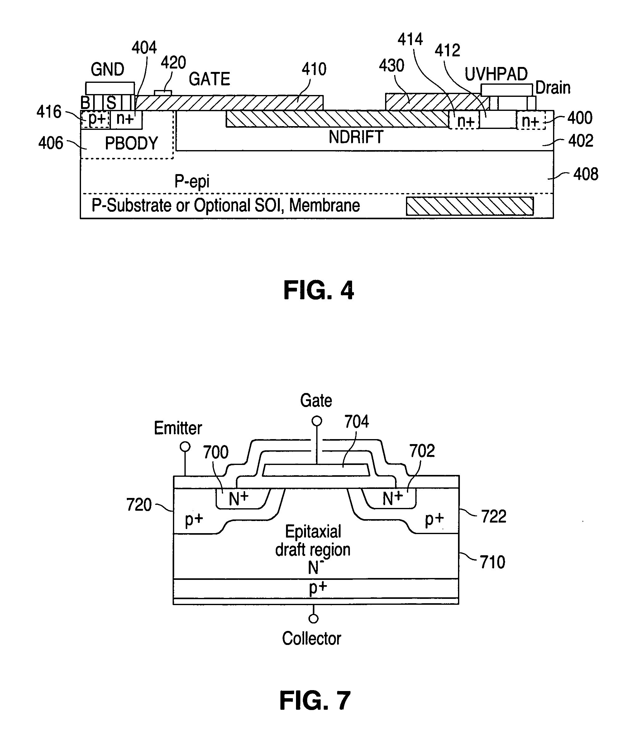
[0016]In contrast to the configuration described above, the LDMOS-SCR-like structure of the invention (that is referred to herein as UHV LDMOS) provides for a symmetrical drift region formed around a central pad defining the drain region of the device. One such embodiment is shown in cross-section in FIG. 4, which shows an n+ drain 400 formed in a long n-drift region 402, which will be discussed in greater detail below. The n+ source 404 is formed in a p-body or p-well 406. The n-drift region 402 and p-body 406 are, in turn formed in a p-epitaxial region 408. A poly gate 410 with gate contact 420 is formed near to the source region, and is spaced fr...
PUM
 Abstract
Description
Claims
Application Information