Pixel electrode panel, a liquid crystal display panel assembly and methods for manufacturing the same

a liquid crystal display panel and electrode panel technology, applied in the direction of instruments, nuclear engineering, transportation and packaging, etc., can solve the problems of reducing the aperture ratio of electric field generating electrodes, rainbow stains may appear on degrading the visibility of the liquid crystal display device, so as to improve the front and side visibilities

Active Publication Date: 2011-10-06
TCL CHINA STAR OPTOELECTRONICS TECH CO LTD
View PDF11 Cites 104 Cited by
  • Summary
  • Abstract
  • Description
  • Claims
  • Application Information

AI Technical Summary

Benefits of technology

[0010]An exemplary embodiment of the present invention provides a pixel electrode panel that improves front and side visibilities.

Problems solved by technology

The slits in the electric field generating electrodes reduce an aperture ratio, however.
However, in the VA mode liquid crystal display device such as the SVA and PVA mode liquid crystal display devices, the contrast ratio is reduced according to an increase in the side viewing angle, and luminance ratios of the primary colors, e.g., red, blue and green, cross each other at a certain gray scale within a particular range, thus degrading visibility of the liquid crystal display device.
In addition, when fluorescent light is incident on a liquid crystal display device, rainbow stains may appear on the liquid crystal display device.

Method used


Image

  • Pixel electrode panel, a liquid crystal display panel assembly and methods for manufacturing the same
  • Pixel electrode panel, a liquid crystal display panel assembly and methods for manufacturing the same
  • Pixel electrode panel, a liquid crystal display panel assembly and methods for manufacturing the same

Examples


Embodiment Construction

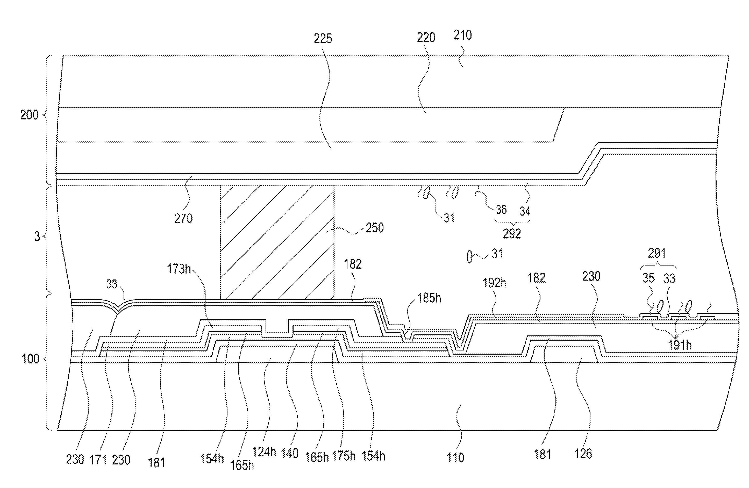
[0092]Exemplary embodiments of the present invention will now be described in detail with reference to the accompanying drawings. The present invention may, however, be embodied in many different forms and should not be construed as being limited to the embodiments set forth herein.

[0093]Throughout the following description and drawings, the same reference numerals may refer to the same components, features and / or structures.

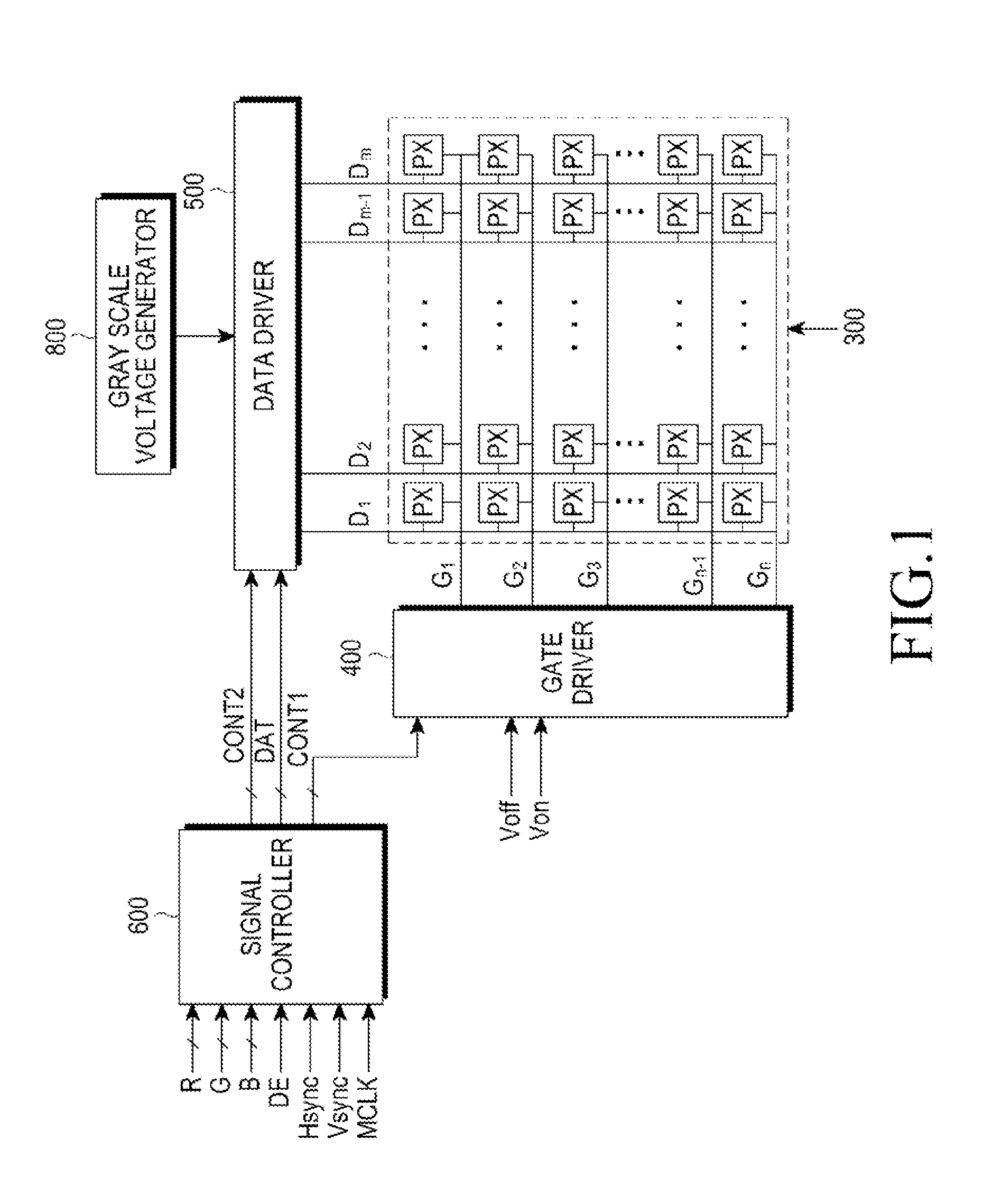
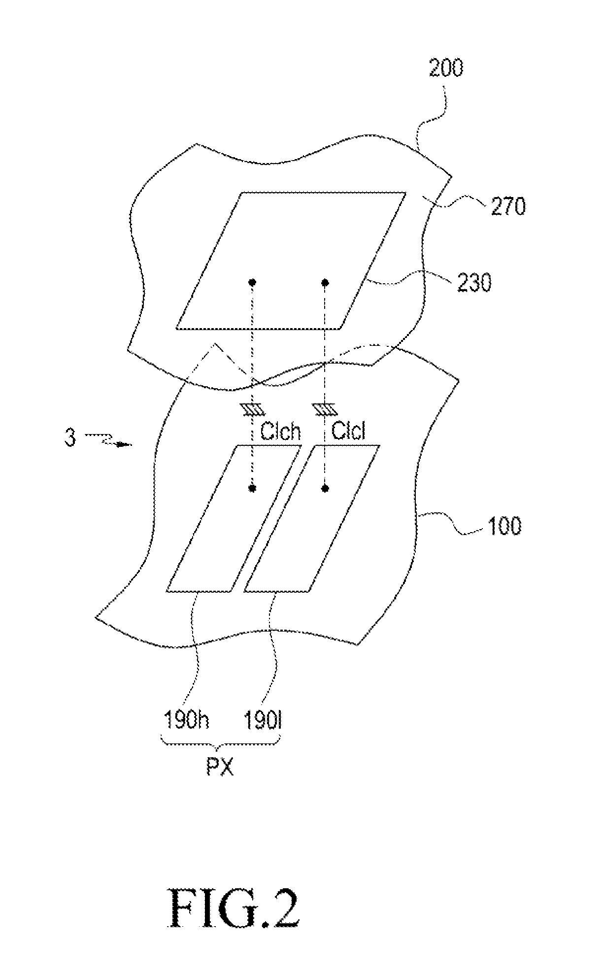
[0094]A liquid crystal display device according to an exemplary embodiment of the present invention will be described in detail with reference to FIGS. 1 and 2. FIG. 1 is a block diagram of a liquid crystal display device according to an exemplary embodiment of the present invention. FIG. 2 schematically illustrates a structure of two subpixels 190h and 190l constituting one pixel PX in a liquid crystal display device according to an exemplary embodiment of the present invention. As illustrated in FIG. 1, a liquid crystal display device includes a liquid crystal...


PUM

PropertyMeasurementUnit
widthsaaaaaaaaaa
widthsaaaaaaaaaa
angleaaaaaaaaaa

Abstract

A liquid crystal display panel, including: a pixel electrode formed on a first substrate; an alignment layer formed on the pixel electrode, wherein the alignment layer includes an alignment layer material and aligns first liquid crystal molecules in a direction substantially perpendicular to the pixel electrode; and a photo hardening layer formed on the alignment layer, wherein the photo hardening layer includes a photo hardening layer material and aligns second liquid crystal molecules to be tilted with respect to the pixel electrode, wherein the alignment layer material and the photo hardening layer material have different polarities from each other.

Description

CROSS-REFERENCE TO RELATED APPLICATIONS[0001]This application claims priority under 35 U.S.C. §119(a) to a Korean Patent Application filed in the Korean Intellectual Property Office on Apr. 2, 2010 and assigned Serial No. 10-2010-0030591, a Korean Patent Application filed in the Korean Intellectual Property Office on May 20, 2010 and assigned Serial No. 10-2010-0047746, a Korean Patent Application filed in the Korean Intellectual Property Office on Jun. 4, 2010 and assigned Serial No. 10-2010-0052878, a Korean Patent Application filed in the Korean Intellectual Property Office on Jul. 16, 2010 and assigned Serial No. 10-2010-0069254 and a Korean Patent Application filed in the Korean Intellectual Property Office on Nov. 30, 2010 and assigned Serial No. 10-2010-0121019, the disclosures of which are incorporated by reference herein in their entireties.BACKGROUND OF THE INVENTION[0002]1. Technical Field[0003]The present invention relates to a pixel electrode panel, a liquid crystal dis...

Claims


Application Information

Patent Timeline
Patent Type & Authority Applications(United States)
IPC IPC(8): G02F1/1337G02F1/1343C08J7/18C08F2/50
CPCC08G8/12C08G73/12G02F1/133707G02F1/133723G02F1/133753G02F2001/133761G02F1/134309G02F1/1393G02F2001/133531G02F2001/133742G02F2001/133746G02F1/133788G02F1/133531G02F1/133742G02F1/133746G02F1/133761
Inventor CHOI, KYONG-SIKPARK, MYUNG-JAEPARK, MIN-WOOKKIM, SUNG-HOONLEE, GAK-SEOKSHIN, WOO-JUNGLEE, JUN-HYUPOH, KEUN-CHANKIM, SANG-GYUNKIM, SU-JEONGPARK, SEUNG-BEOMJEONG, YOUN-HAK
Owner TCL CHINA STAR OPTOELECTRONICS TECH CO LTD
Why Eureka
Try Eureka