
Liquid crystal display device and method of manufacturing the same

a technology of liquid crystal display and display device, which is applied in the direction of non-linear optics, instruments, optics, etc., can solve the problems of inability to control the formation of defect holes in the substrate, the pattern of each of the function layers may become defective during the fabrication of each of the function layers, and the substrate with reduced thickness may be undetected damage or deformed. , to achieve the effect of reducing the amount of diffused reflection

Inactive Publication Date: 2011-10-27
SAMSUNG DISPLAY CO LTD
View PDF5 Cites 2 Cited by
  • Summary
  • Abstract
  • Description
  • Claims
  • Application Information

AI Technical Summary

Benefits of technology

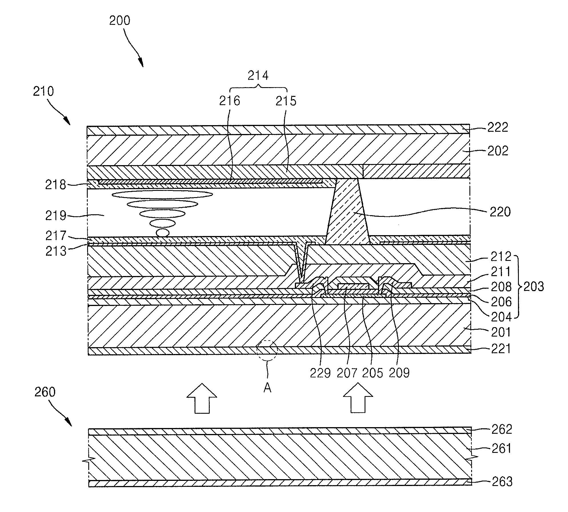
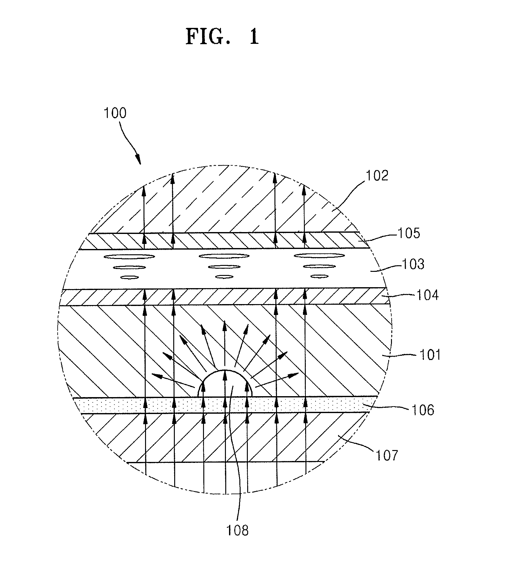
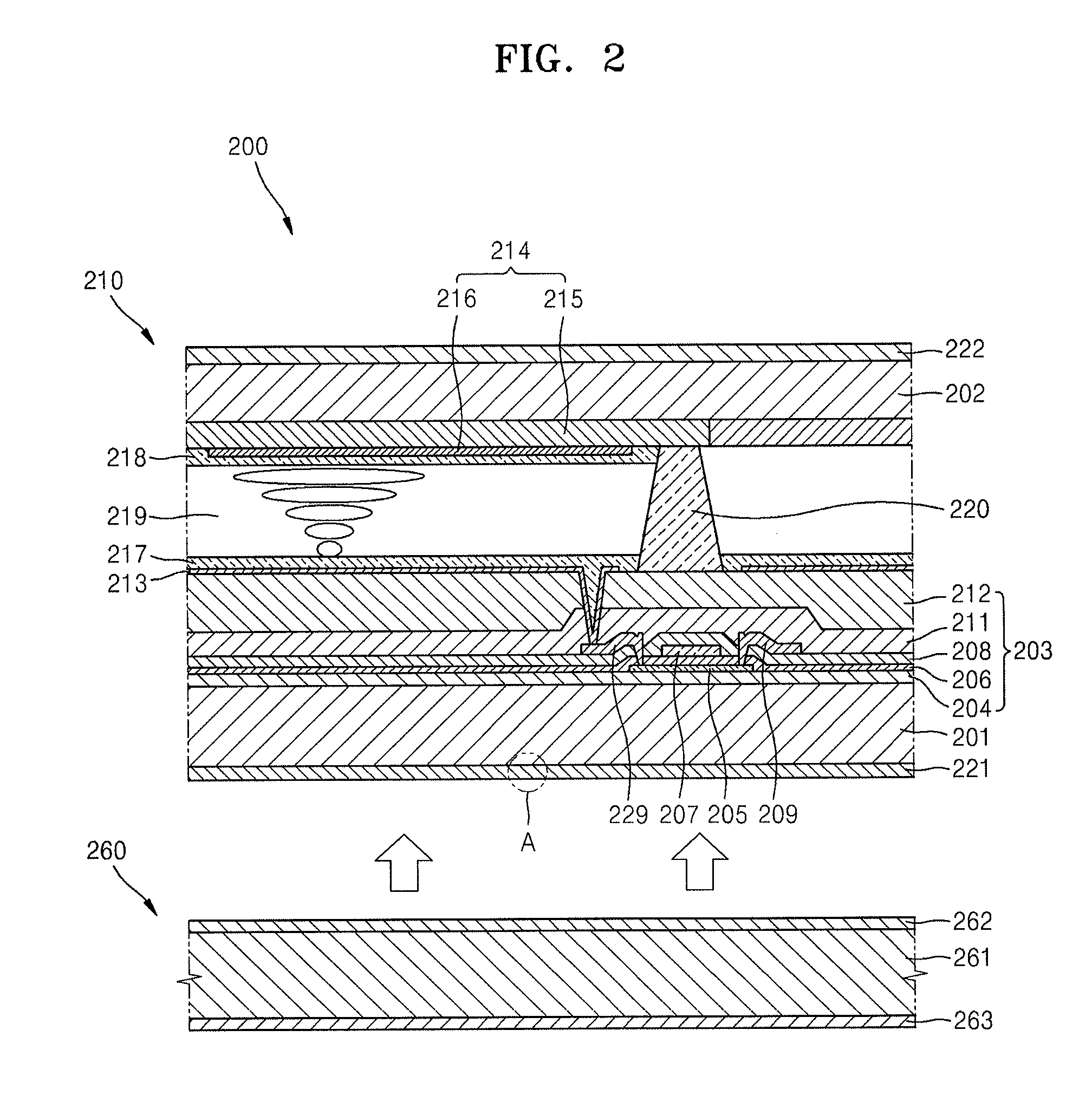
[0014]It is a feature of an embodiment to provide a liquid crystal display device in which diffused-reflection is reduced by filling defect holes on a substrate with a filling.

Problems solved by technology

However, if each function layer is formed on the substrates after the thicknesses of the substrates are reduced, the substrates with reduced thicknesses may be undesirably damaged or deformed.
In addition, patterns of each of the function layers may become defective during fabrication of each of the function layers, e.g., by a baking process at a high temperature.
However, if the substrates are etched by using a conventional etching solution, it may be difficult to control formation of defect holes in the substrates.
However, there is a limit to reducing the polished thickness of an etched substrate when the etched substrate is polished by using a polisher.
Therefore, defect holes may remain in the substrate.
Especially, in mass production, defect holes may be scattered throughout a plurality of substrates, and thus it is difficult to select substrates to be polished.
Furthermore, compared to the recent trend of reducing a thickness of a substrate, sizes of defect holes are increasing.
Therefore, the probability of defects further increases.

Method used


Image

  • Liquid crystal display device and method of manufacturing the same
  • Liquid crystal display device and method of manufacturing the same
  • Liquid crystal display device and method of manufacturing the same

Examples


Embodiment Construction

[0039]Korean Patent Application No. 10-2010-0038098, filed on Apr. 23, 2010, in the Korean Intellectual Property Office, and entitled: “Liquid Crystal Display Device and Method of Manufacturing the Same,” is incorporated by reference herein in its entirety.

[0040]Example embodiments will now be described more fully hereinafter with reference to the accompanying drawings; however, they may be embodied in different forms and should not be construed as limited to the embodiments set forth herein. Rather, these embodiments are provided so that this disclosure will be thorough and complete, and will fully convey the scope of the invention to those skilled in the art.

[0041]In the drawing figures, the dimensions of layers and regions may be exaggerated for clarity of illustration. It will also be understood that when a layer or element is referred to as being “on” another layer or substrate, it can be directly on the other layer or substrate, or intervening layers may also be present. In ad...


PUM

PropertyMeasurementUnit
depthsaaaaaaaaaa
sizesaaaaaaaaaa
refractive indexaaaaaaaaaa

Abstract

A liquid crystal display device and a method of manufacturing the same, the device including a liquid crystal display panel, the liquid crystal display panel including substrates facing each other and a liquid crystal layer therebetween; a backlight unit below the liquid crystal display panel, the backlight unit being for emitting light toward the liquid crystal display panel; a filling that fills defect holes on surfaces of the substrates, which surfaces are relatively remote from the liquid crystal layer, the filling having horizontally even surfaces with respect to the surfaces of the substrates, and a cover member disposed over the defect holes filled with the filling.

Description

BACKGROUND[0001]1. Field[0002]Embodiments relate to a liquid crystal display device and a method of manufacturing the same.[0003]2. Description of the Related Art[0004]Generally, a liquid crystal display panel is a light receiving type display device that forms an image with external light incident thereon.[0005]Since a liquid crystal display panel cannot emit light by itself, a backlight unit may be installed behind the liquid crystal display panel and may irradiate light toward the panel. Therefore, an image may be viewed even in a dark location. A backlight unit may also be used as a surface light source device, e.g., an illuminated signboard.[0006]A liquid crystal display panel may include liquid crystal between two substrates. When power is supplied, the liquid crystal display panel may display, e.g., images, numbers, and texts, by rearranging liquid crystal molecules. Liquid crystal display panels may be categorized into various types based on driving mechanisms, displaying me...

Claims


Application Information

Patent Timeline
Patent Type & Authority Applications(United States)
IPC IPC(8): G02F1/1335
CPCG02F2001/133302G02F1/1309G02F1/133302
Inventor KIM, DO-HYUN
Owner SAMSUNG DISPLAY CO LTD
Learn More