Semiconductor device for preventing crack in pad region and fabricating method thereof

Active Publication Date: 2011-11-10
KEY FOUNDRY CO LTD
View PDF5 Cites 12 Cited by
  • Summary
  • Abstract
  • Description
  • Claims
  • Application Information

AI Technical Summary

Benefits of technology

[0008]Aspects of the present invention relate to a semiconductor device which p

Problems solved by technology

As a result, mechanical stress occurs on the pad region and if the stress exceeds a certain level, a crack appears on the pad region.
Accordingly, cracks occur more frequently

Method used


Image

  • Semiconductor device for preventing crack in pad region and fabricating method thereof
  • Semiconductor device for preventing crack in pad region and fabricating method thereof
  • Semiconductor device for preventing crack in pad region and fabricating method thereof

Examples


Example

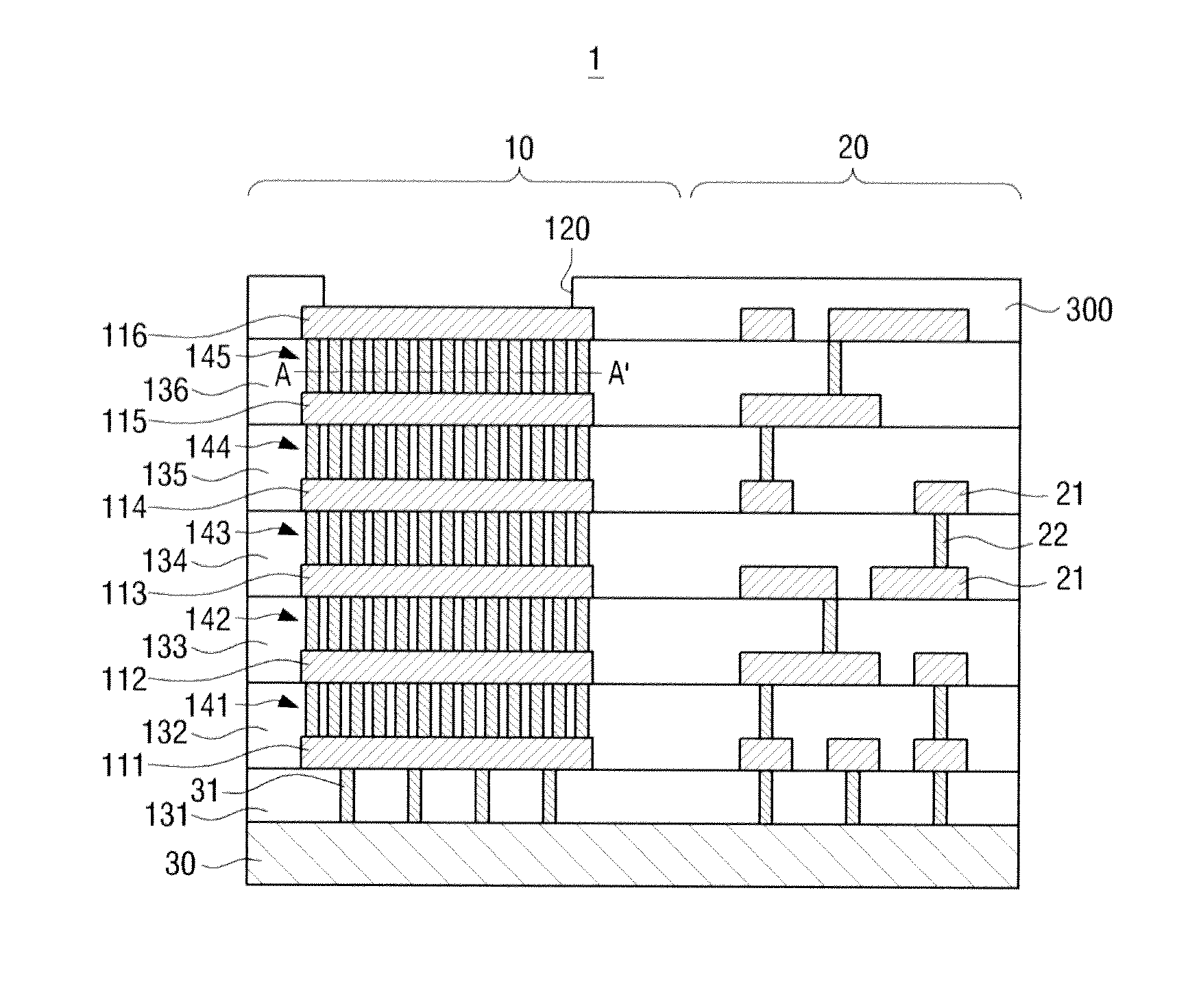
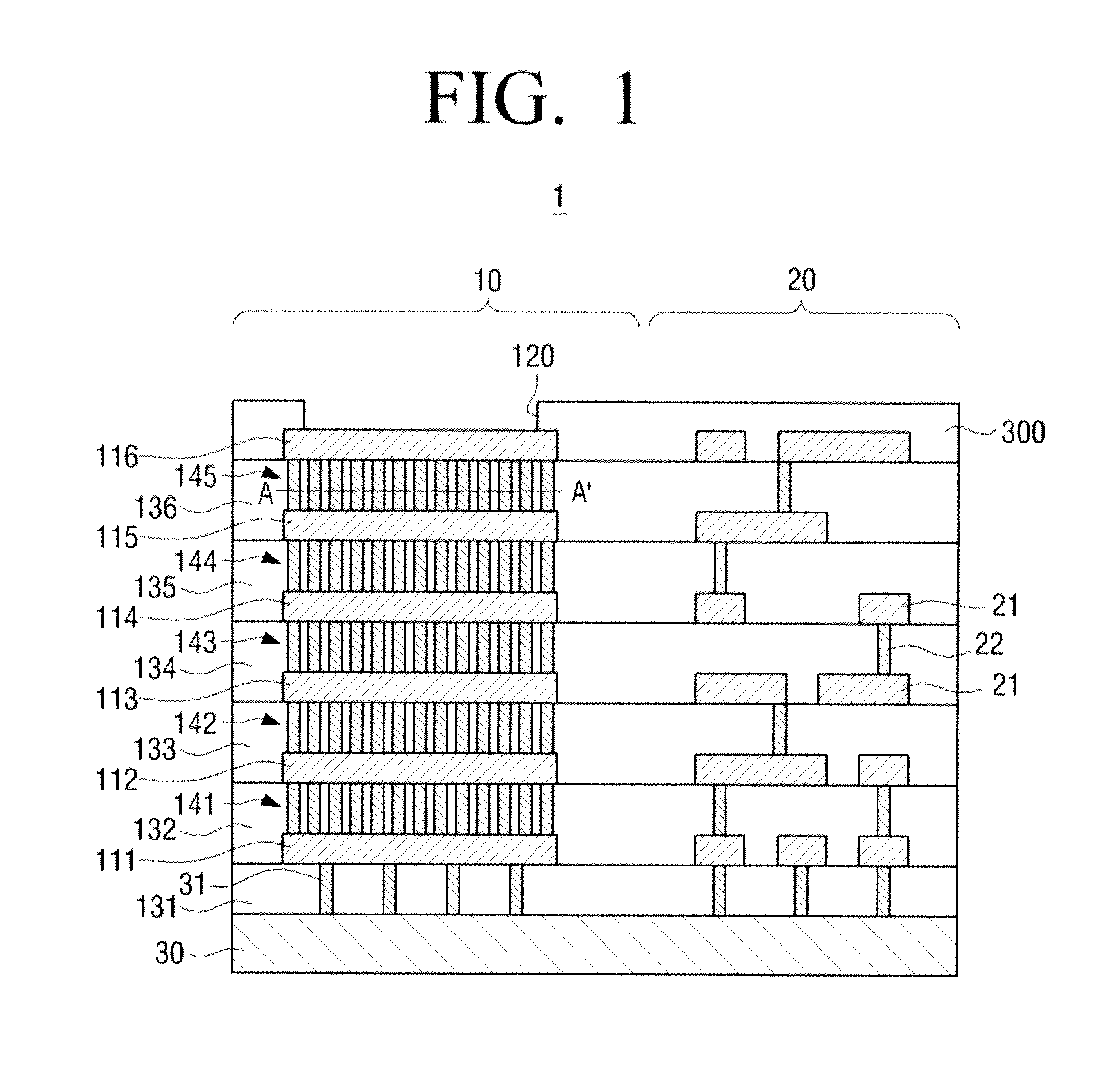
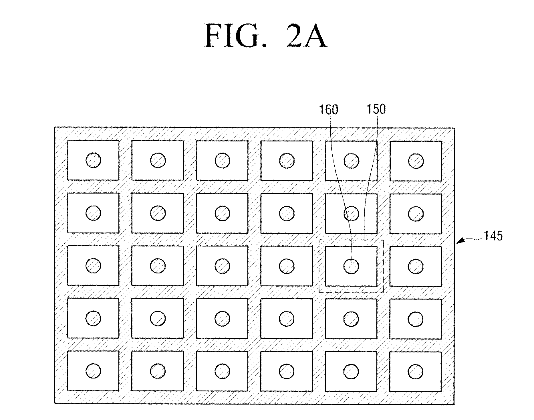
[0036]Certain exemplary embodiments are described in greater detail below with reference to the accompanying drawings.

[0037]In the following description, like drawing reference numerals are used for the like elements, even in different drawings. The matters defined in the description, such as detailed construction and elements, are provided to assist in a comprehensive understanding of exemplary embodiments. However, exemplary embodiments can be practiced without those specifically defined matters. Also, well-known functions or constructions are not described in detail since they would obscure the application with unnecessary detail.

[0038]In order to provide better understanding of the invention, the views illustrating exemplary embodiments are not drawn on an actual scale, and measurements of some elements may be exaggerated. In addition, the positions of a certain layer or regions in the views indicate only relative positions, and the third layer or region may exist between layers...


PUM


Abstract

A semiconductor device which prevents a crack from occurring on a pad region is provided. The semiconductor device includes a lower pad, an upper pad which is formed above the lower pad, an insulation layer which is formed between the lower pad and the upper pad, a via net for electrically connecting the lower pad and the upper pad in the insulation layer, the via net having a net shape in which a unit grid is connected with its adjacent unit grids to form a net structure, and at least one via hole for electrically connecting the lower pad and the upper pad in the unit grid of the via net.

Description

CROSS-REFERENCE TO RELATED APPLICATIONS[0001]This application claims priority from Korean Patent Application No. 2010-43415, filed in the Korean Intellectual Property Office on May 10, 2010, the disclosure of which is incorporated herein by reference.BACKGROUND OF THE INVENTION[0002]1. Field of he Invention[0003]Aspects of the present invention relate to a semiconductor device, and more particularly, to a semiconductor device which prevents a crack from occurring on a pad region and a fabricating method thereof.[0004]2. Description of the Prior Art[0005]Generally, a semiconductor device has a pad region which connects an integrated circuit with a package, and the pad region is often pressured by external force in the process of wire-bonding or probing. For instance, a certain pressure is applied to the pad region while the pad is connected to a lead during wire-bonding, and the needle of a probe applies certain pressure on the pad region during probing. As a result, mechanical stres...

Claims


Application Information

Patent Timeline
IPC IPC(8): H01L23/522H01L21/768
CPCH01L23/585H01L2224/02166H01L24/05H01L2224/04042H01L2224/05096H01L2224/05624H01L2224/05666H01L2224/45144H01L2224/45147H01L2924/01013H01L2924/01029H01L2924/01033H01L2924/01079H01L2924/01082H01L2924/0105H01L2924/01074H01L2224/48624H01L2224/48666H01L2224/48866H01L24/04H01L2224/48824H01L2924/00H01L23/48H01L23/492H01L24/06H01L2224/02123H01L2924/14H01L2924/00014H01L2224/05094H01L2224/05011H01L2224/05083H01L2224/05093H01L21/76877H01L23/5226H01L23/528H01L24/03
Inventor JEONG, JONG-YEUL
Owner KEY FOUNDRY CO LTD
Why Eureka
Try Eureka