Thin channel device and fabrication method with a reverse embedded stressor

Inactive Publication Date: 2011-12-01
ALSEPHINA INNOVATIONS INC
View PDF4 Cites 29 Cited by
  • Summary
  • Abstract
  • Description
  • Claims
  • Application Information

AI Technical Summary

Problems solved by technology

However, embedded stressors, such as SiGe or Si:C, which are usually employed in bulk and partially depleted (PD) SOI technologies to improve device performance cannot be used with thin channel structures.
An embedded stressor structure for bulk devices, is not suitable for thin-channel devices because the total channel thickness is limited to control electrostatic integrity of the device.
Present embedded stressors cannot be used with a thin-channel MOSFET structure since a total semiconductor thickness is limited among other things.

Method used


Image

  • Thin channel device and fabrication method with a reverse embedded stressor
  • Thin channel device and fabrication method with a reverse embedded stressor
  • Thin channel device and fabrication method with a reverse embedded stressor

Examples


Embodiment Construction

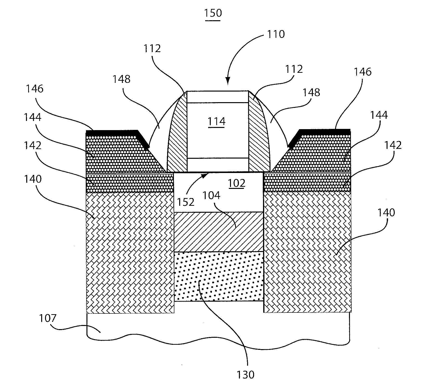
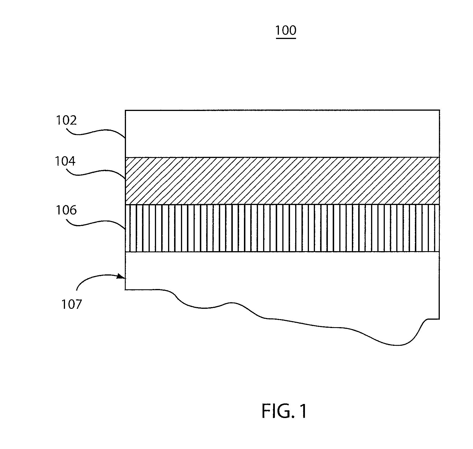
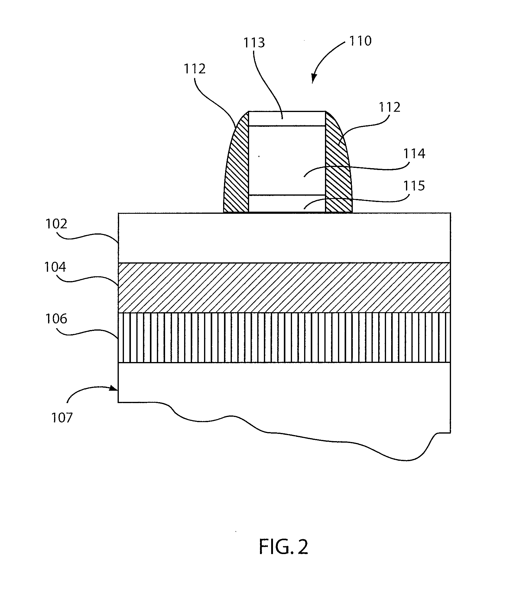
[0019]In accordance with the present principles, a device structure for thin-channel devices, such as thin-channel metal oxide semiconductor field effect transistors (MOSFETs), includes a reverse embedded stressor under a thin buried oxide. In addition, a method to fabricate this structure is disclosed. Advantageously, device electrostatics are controlled by channel thickness, while channel stress is provided from the buried reverse embedded stressor.

[0020]It is to be understood that the present invention will be described in terms of a given illustrative architecture; however, other architectures, structures, substrate materials and process features and steps may be varied within the scope of the present invention.

[0021]A circuit formed from the devices as described herein may be part of a design for an integrated circuit chip. The chip design may be created in a graphical computer programming language, and stored in a computer storage medium (such as a disk, tape, physical hard dr...


PUM


Abstract

A device and method for inducing stress in a semiconductor layer includes providing a substrate having a dielectric layer formed between a first semiconductor layer and a second semiconductor layer. A removable buried layer is provided on or in the second semiconductor layer. A gate structure with side spacers is formed on the first semiconductor layer. Recesses are formed down to the removable buried layer in areas for source and drain regions. The removable buried layer is etched away to form an undercut below the dielectric layer below the gate structure. A stressor layer is formed in the undercut, and source and drain regions are formed.

Description

BACKGROUND[0001]1. Technical Field[0002]The present invention relates to semiconductor devices and fabrication, and more particularly to a thin channel device and fabrication method that employs an embedded stressor layer.[0003]2. Description of the Related Art[0004]Thin channel metal oxide semiconductor field effect transistors (MOSFETs), such as ultrathin body semiconductor-on-insulators (SOI), FinFETs, trigates, or nanowire structures may be candidates for device scaling in 22 nm node and beyond. However, embedded stressors, such as SiGe or Si:C, which are usually employed in bulk and partially depleted (PD) SOI technologies to improve device performance cannot be used with thin channel structures. An embedded stressor structure for bulk devices, is not suitable for thin-channel devices because the total channel thickness is limited to control electrostatic integrity of the device. Present embedded stressors cannot be used with a thin-channel MOSFET structure since a total semico...

Claims


Application Information

Patent Timeline
IPC IPC(8): H01L29/786H01L21/336
CPCH01L21/26506H01L29/66772H01L29/78654H01L29/785H01L29/7849
Inventor CHENG, KANGGUODORIS, BRUCE B.KHAKIFIROOZ, ALIKULKARNI, PRANITASHAHIDI, GHAVAM G.
Owner ALSEPHINA INNOVATIONS INC
Why Eureka
Try Eureka