Pin card and test apparatus using the same

a test apparatus and pin card technology, applied in the field of pin cards, can solve the problems of high cost of mems switches, the inability of composite semiconductor switches to handle test patterns including dc components, and the cost of such switches is almost 100 times that of other switches

Active Publication Date: 2011-12-01
ADVANTEST CORP
View PDF2 Cites 5 Cited by
  • Summary
  • Abstract
  • Description
  • Claims
  • Application Information

AI Technical Summary

Benefits of technology

[0015]The present invention has been made in view of such a situation. Accordingly, it is an exemplary purpose of the present invention to provide a pin card employing low-cost switches.
[0020]By providing the first inductor and the second inductor, such an arrangement provides increased impedance of a path including the first switch SW1. With such an arrangement, only signals having a very low frequency pass through the first switch SW1 side, and signals having other frequencies pass through the bypass capacitor side. Thus, such an arrangement reduces the crossover frequency of a path that includes the first switch and a path that includes the bypass capacitor, thereby reducing the level of difficulty in the design. It should be noted that examples of inductors include a ferrite bead inductor.

Problems solved by technology

However, such a composite semiconductor switch has a very low DC breakdown voltage on the order of 0.1 V. Accordingly, such a composite semiconductor switch cannot be used to handle a test pattern including a DC component.
Moreover, although such a MEMS switch satisfies the requirements of such high-speed operation and sufficient DC breakdown voltage, such a MEMS switch has a problem of a high cost.
Specifically, the cost of such a MEMS switch is almost 100 times that of other switches.
Accordingly, if MEMS switches are employed in such a test apparatus, it has a strong impact on the cost of the test apparatus.

Method used


Image

  • Pin card and test apparatus using the same
  • Pin card and test apparatus using the same
  • Pin card and test apparatus using the same

Examples


Embodiment Construction

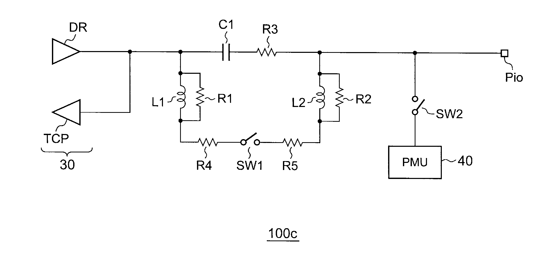
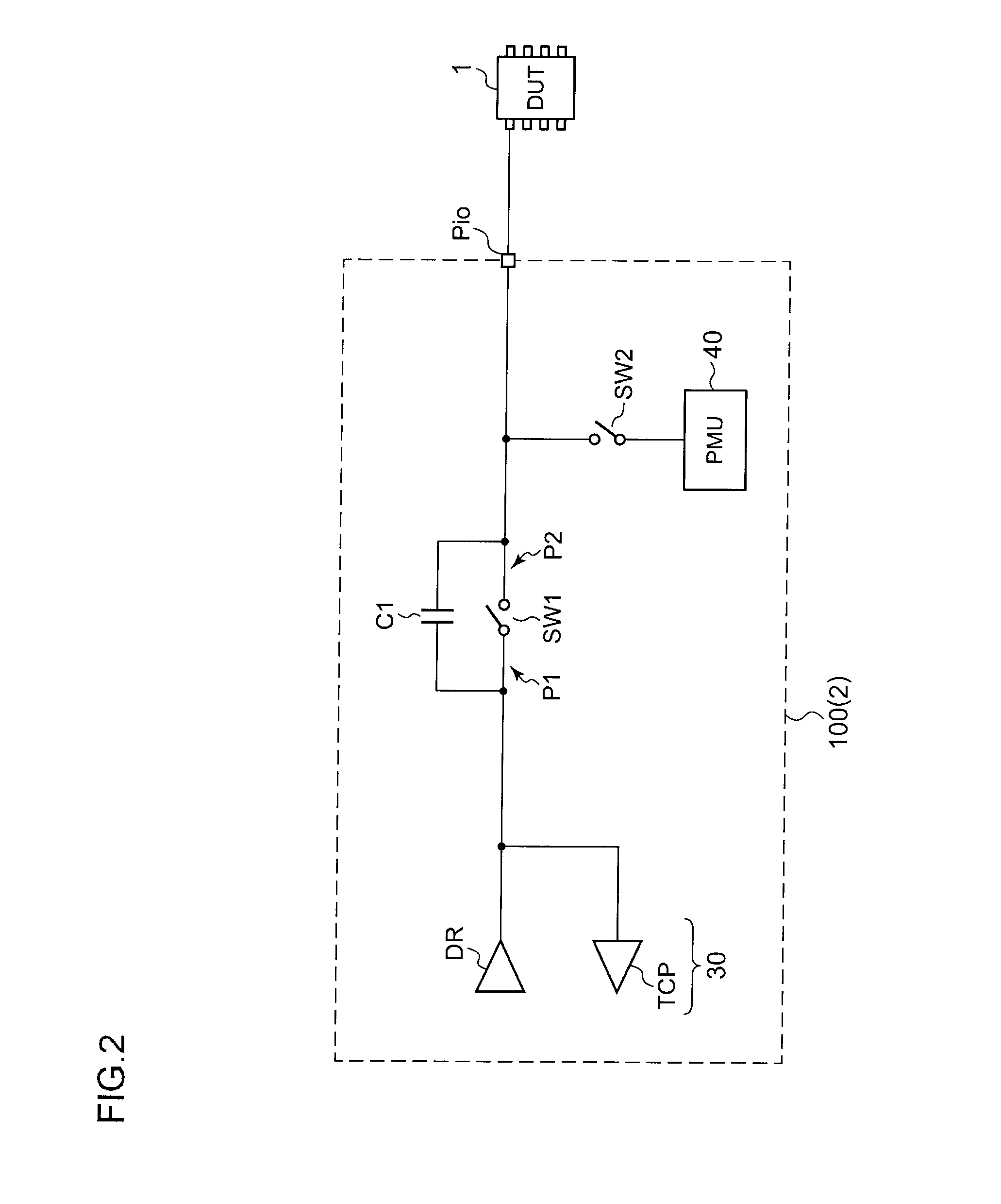
[0036]Description will be made below regarding preferred embodiments according to the present invention with reference to the drawings. The same or similar components, members, and processes are denoted by the same reference numerals, and redundant description thereof will be omitted as appropriate. The embodiments have been described for exemplary purposes only, and are by no means intended to restrict the present invention. Also, it is not necessarily essential for the present invention that all the features or a combination thereof be provided as described in the embodiments.

[0037]In the present specification, a state represented by the phrase “the member A is connected to the member B” includes a state in which the member A is indirectly connected to the member B via another member that does not affect the electric connection therebetween, in addition to a state in which the member A is physically and directly connected to the member B. Similarly, a state represented by the phra...


PUM


Abstract

A first switch is arranged such that a first terminal thereof is connected to an AC test unit and a second terminal thereof is connected to an I / O terminal and a DC test unit. A first switch is configured so as to be capable of switching states between a connection state in which the first terminal and the second terminal are connected to each other, and a disconnection state in which they are disconnected from each other. A bypass capacitor is arranged between the first terminal and the second terminal, and is configured to bypass the frequency component which is cut off by the first switch.

Description

CROSS REFERENCE TO RELATED APPLICATIONS[0001]This application is the U.S. National Stage of International Patent Application No. PCT / JP2010 / 002901 filed on Apr. 22, 2010, the disclosure of which is hereby incorporated by reference in its entirety.BACKGROUND OF THE INVENTION[0002]1. Field of the Invention[0003]The present invention relates to a pin card.[0004]2. Description of the Related Art[0005]A semiconductor test apparatus (which will be referred to simply as the “test apparatus” hereafter) is used to test whether or not a semiconductor device operates normally or to identify defective parts. A typical test apparatus performs an AC test operation and a DC test operation.[0006]In the AC test operation, a test pattern is generated by a pattern generator and a timing generator, and a driver supplies the test pattern thus generated to a device under test (DUT). Upon receiving the pattern signal, the DUT performs predetermined signal processing, and outputs an output signal to the te...

Claims


Application Information

Patent Timeline
Patent Type & Authority Applications(United States)
IPC IPC(8): G01R1/067
CPCG01R31/2851G01R31/2841
Inventor KAWAHARA, TAKAONAKAMURA, TAKAYUKI
Owner ADVANTEST CORP
Why Eureka
Try Eureka