Semiconductor device

a technology of semiconductor devices and semiconductors, applied in semiconductor devices, semiconductor/solid-state device details, electrical apparatus, etc., can solve problems such as cracks in the dicing region, and achieve the effect of effectively preventing the noise transmission between the first device region and the second device region, reducing the total capacity c, and increasing the impedance z suitably

Active Publication Date: 2006-05-18
RENESAS ELECTRONICS CORP
View PDF34 Cites 72 Cited by
  • Summary
  • Abstract
  • Description
  • Claims
  • Application Information

AI Technical Summary

Benefits of technology

[0028] An example of the above (ii) is a configuration that near the surface of a semiconductor substrate, a diffusion layer having an opposite conductivity type to that of the semiconductor substrate is provided; a guard ring is connected to the surface of the semiconductor substrate in the region comprising the diffusion layer having the opposite conductivity type; and a junction plane in the diffusion layer constitutes a nonconducting part. Herein, in accordance with equation (1), C can be reduced to suitably increase Z. Thus, noise transmission between the first device region and the second device region can be effectively prevented. An impurity concentration profile in the diffusion layer with an opposite conductivity type may be selected from various types without any particular restrictions.
[0029] The aspect of the above (ii) is particularly effective for a configuration that an analog and a digital circuit devices are formed in either the first device region or the second device region. In such a configuration, when a noise generated in the digital circuit device is transmitted through the above path, an impedance Z can be suitably increased by effectively reducing the total capacity C in the path. When o is small in equation (1), such an effect can be more significant, to effectively prevent transmission of a low-frequency noise.
[0030] As described above, the present inventor has found that a noise generated in a certain device region is transmitted to another device region through a guard ring such as a seal ring, causing, for example, malfunction in a device in the other device region. In this invention, a nonconducting part is formed in a guard ring forming region. The nonconducting part blocks conduction in a path from the first device region, through the guard ring to the second device region, so that noise transmission between the first and the second device regions can be reliably prevented.
[0031] Thus, according to this invention, noise transmission through a guard ring intervening between two device regions can be effectively prevented.

Problems solved by technology

During dicing, cracks may occur in the dicing region.

Method used


Image

  • Semiconductor device
  • Semiconductor device
  • Semiconductor device

Examples


embodiment 1

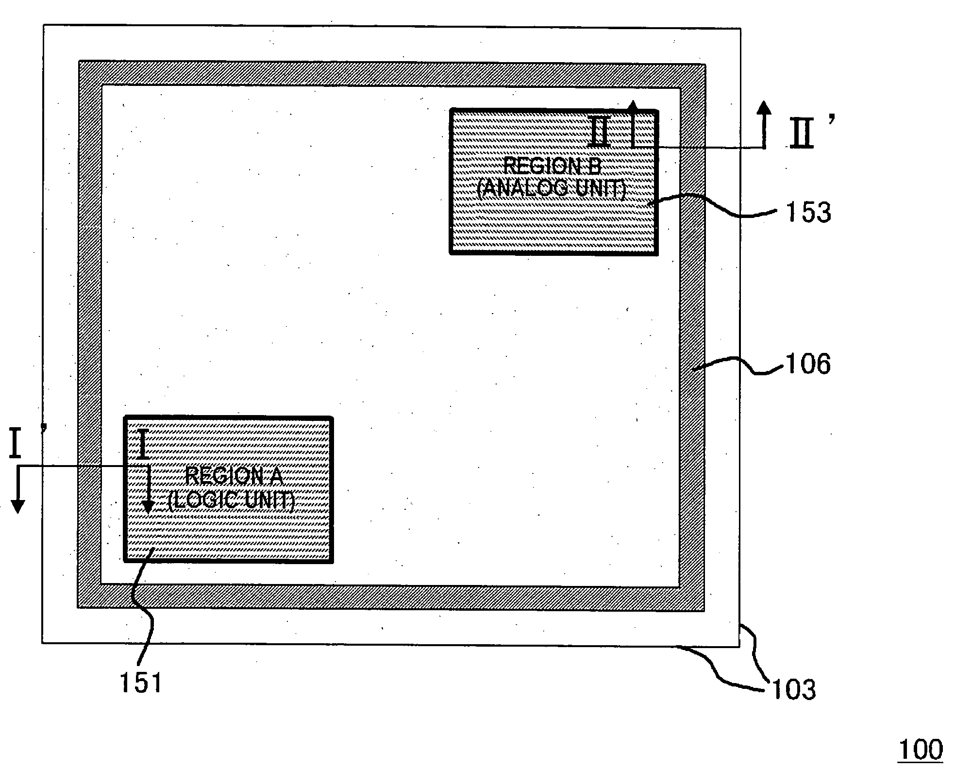
[0048]FIG. 1 is a plan view showing a configuration of a semiconductor chip in this embodiment. A semiconductor chip 100 shown in FIG. 1 includes two device regions, that is, a logic unit 151 (region A) and an analog unit 153 (region B) in a silicon substrate 101. The semiconductor chip 100 includes a annular seal ring region 106 surrounding these device regions along a dicing plane 103. There will be described an exemplary configuration where a seal ring 105 (FIGS. 2 and 3) formed in the seal ring region 106 is comprised of a triple-layered annular conductive plug.

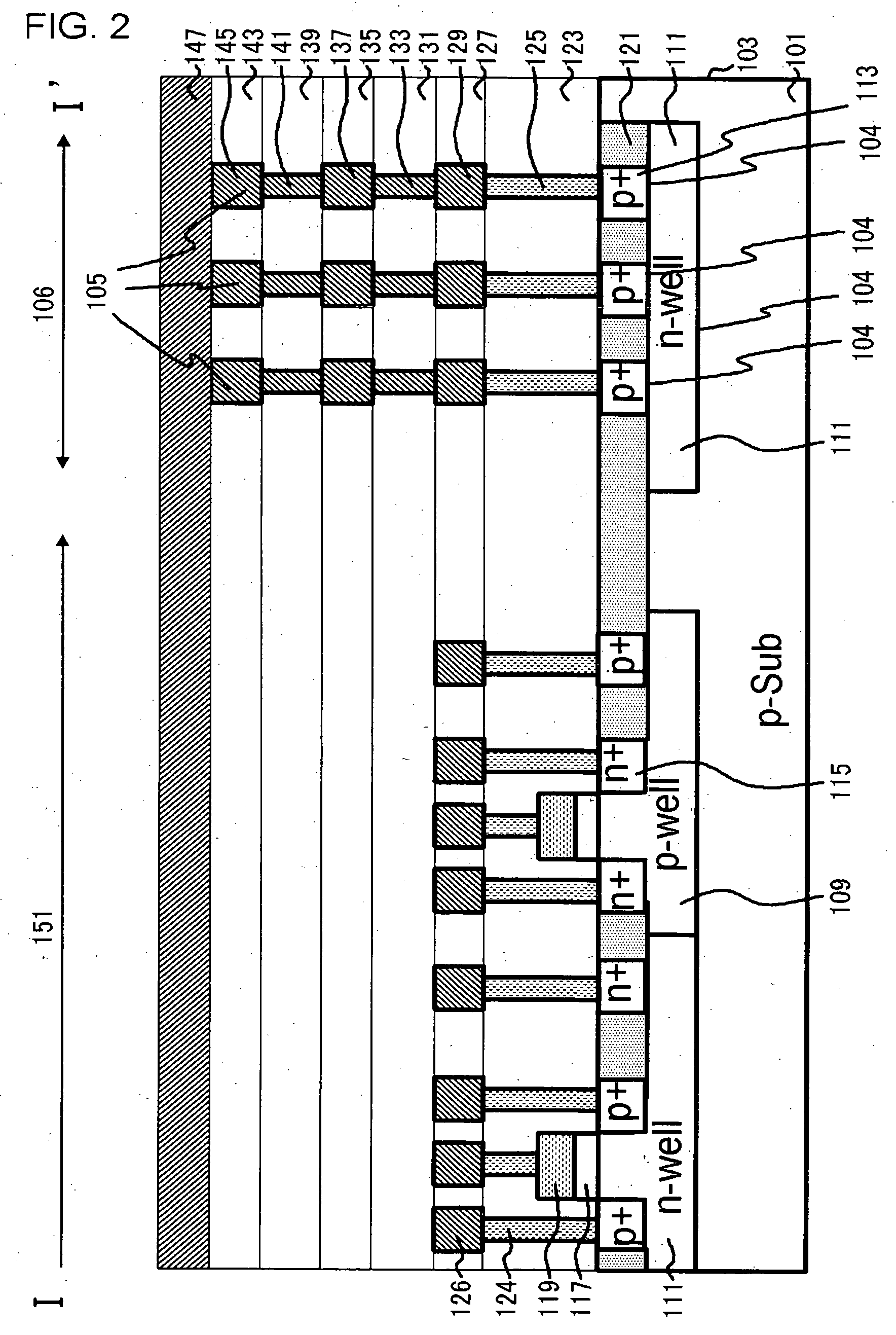
[0049]FIG. 2 is a cross-sectional view taken on line I-I′ of FIG. 1, and FIG. 3 is a cross-sectional view taken on line II-II′ of FIG. 1. Each of FIGS. 2 and 3 shows a configuration of the seal ring region 106 and an internal circuit adjacent to the region.

[0050] The semiconductor chip 100 shown in FIGS. 1 to 3 is a semiconductor device comprising the first and the second device regions (the logic unit 151 and the analo...

embodiment 2

[0093] In the semiconductor chip described in Embodiment 1, the seal ring region 106 may have the following cross-sectional structure. In this embodiment, a planar configuration in the semiconductor chip may be also as described with reference to FIG. 1. FIG. 4 is a cross-sectional view showing a configuration of the semiconductor device according to this embodiment. Although FIG. 4 shows a cross-sectional view taken on line II-II′ of FIG. 1 which corresponds to FIG. 3 in Embodiment 1, the I-I′ cross-section may have the configuration in FIG. 4, in which the analog unit 153 in FIG. 4 is the logic unit 151.

[0094] As shown in FIG. 4, the semiconductor device of this embodiment includes a diffusion layer (an n+-diffusion layer 115 and an n-well 111) with an opposite conductivity type to that of a silicon substrate 101 near the surface of the silicon substrate, and a seal ring 105 is connected to the surface of the n+-diffusion layer 115. Furthermore, a junction plane in the n-well 111...

embodiment 3

[0102] In the semiconductor chip described in Embodiment 1, the seal ring region 106 may have the following cross-sectional configuration. Again, in this embodiment, a planar configuration of the semiconductor chip is as described with reference to FIG. 1. FIG. 5 is a cross-sectional view showing the configuration of the semiconductor device according to this embodiment. Although FIG. 5 shows a cross-sectional view taken on line II-II′ of FIG. 1 which corresponds to FIG. 3 in Embodiment 1, the I-I′ cross-section may have the configuration in FIG. 5, in which the analog unit 153 in FIG. 5 is the logic unit 151.

[0103] As shown in FIG. 5, in the semiconductor device of this embodiment, seal ring region 106 has a basic configuration as described for the semiconductor chip in Embodiment 2, except that an n-well 111 is not formed in a silicon substrate 101.

[0104] Again, in this embodiment, the bottom of the seal ring 105, that is, the bottom of the first conductive ring 125 is in contac...


PUM


Abstract

A semiconductor chip 100 includes a logic unit and an analog unit 153. Furthermore, the semiconductor chip 100 includes a silicon substrate 101; a first insulating film 123 to a sixth insulating film 143 formed on the silicon substrate 101; and an annular seal ring 105 consisting of a first conductive ring 125 to a sixth conductive ring 145 buried in the first insulating film 123 to the sixth insulating film 143, which surrounds the periphery of the logic unit and the analog unit 153. In the seal ring region 106, there is formed a pn junction acting as a nonconducting part 104, which blocks conduction in a path from the logic unit, through the seal ring 105 to the analog unit 153.

Description

[0001] This application is based on Japanese patent application NO. 2004-332349, the content of which is incorporated hereinto by reference. BACKGROUND [0002] 1. Technical Field [0003] This invention relates to a semiconductor device comprising a plurality of device regions. [0004] 2. Related Art [0005] In order to protect a circuit-forming region in a semiconductor device from moisture or ions in an external atmosphere, a protective structure which is called a “seal ring” is provided inside of a dicing line, that is, in the vicinity of an edge of a chip (die). The seal ring consists of an interconnect layer (Cu) and a contact as in a circuit-forming region, and is formed such that it surrounds the circuit-forming region in the semiconductor device. [0006] The seal ring can also prevent cracks in the circuit-forming region during dicing the dicing region. During dicing, cracks may occur in the dicing region. However, the seal ring between the dicing region and the circuit-forming re...

Claims


Application Information

Patent Timeline
Patent Type & Authority Applications(United States)
IPC IPC(8): H01L29/00
CPCH01L21/823878H01L23/585H01L27/092H01L29/78H01L2924/3011H01L2924/0002H01L2924/00
Inventor NAKASHIBA, YASUTAKA
Owner RENESAS ELECTRONICS CORP
Why Eureka
Try Eureka