Liquid crystal display device associated with touch panel

Active Publication Date: 2011-12-15
LG DISPLAY CO LTD
View PDF11 Cites 92 Cited by
  • Summary
  • Abstract
  • Description
  • Claims
  • Application Information

AI Technical Summary

Benefits of technology

[0035]An object of the present invention is to provide a liquid crystal display device associated with a touch panel in which a shielding electrode is formed on the rea

Problems solved by technology

Further, if electrodes are formed on both surfaces of the touch panel glass substrate 70, the touch panel glass substrate 70 needs to be turned over during processes, and thereby, process time is increased and occurrence of process defects, such as generation of scratches or foreign substances, is also increased.
The above-described general liquid crystal display device wit

Method used


Image

  • Liquid crystal display device associated with touch panel
  • Liquid crystal display device associated with touch panel
  • Liquid crystal display device associated with touch panel

Examples


first embodiment

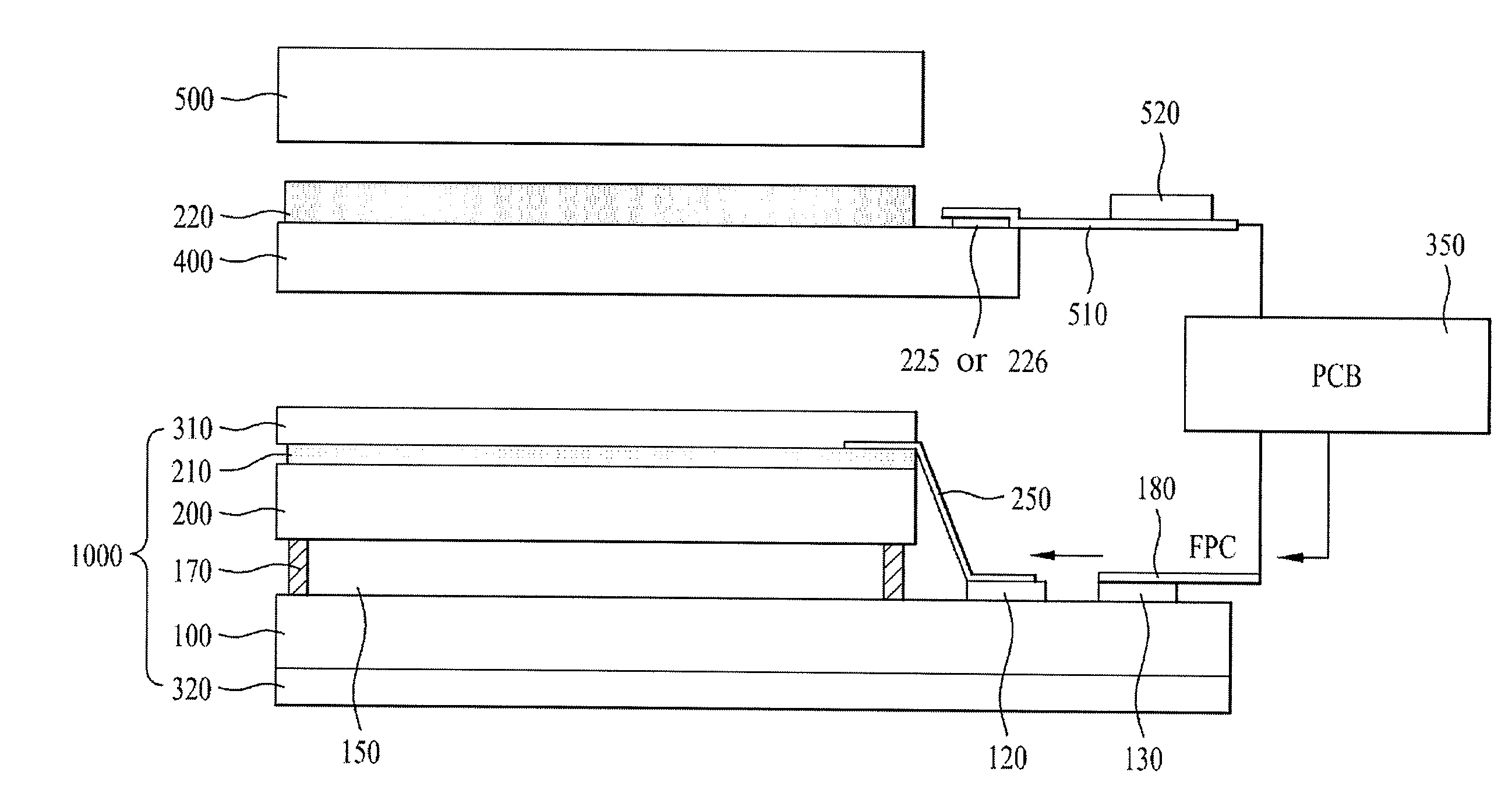
[0062]FIG. 3 is a longitudinal-sectional view of a liquid crystal display device associated with a touch panel in accordance with the present invention.

[0063]The liquid crystal display device in accordance with the first embodiment of the preset invention includes a main panel including a thin film transistor array substrate 100 and a color filter array substrate 200 positioned opposite to each other and a liquid crystal layer 150 formed between the thin film transistor array substrate 100 and the color filter array substrate 200, a shielding electrode 210 formed throughout the entire rear surface of the color filter array substrate 200, a first polarizing plate 310 formed on the rear surface of the color filter array substrate 200 including the shielding electrode 210, a third substrate 400 formed above the first polarizing plate 310 and provided with a sensing unit 220 including intersecting first and second electrodes formed on the upper surface thereof, a touch FPC 510 formed at...

second embodiment

[0079]FIG. 4 is a longitudinal-sectional view of a liquid crystal display device associated with a touch panel in accordance with the present invention.

[0080]The liquid crystal display device in accordance with the second embodiment of the preset invention, as shown in FIG. 4, achieves electrical connection between the shielding electrode 210 and the ground pad electrode 120 through an Ag dot 550, and other parts in this embodiment are substantially the same as those in the first embodiment, and thus a detailed description of a part of the construction and operation of the second embodiment which are substantially the same as those of the first embodiment will be omitted because it is considered to be unnecessary.

[0081]In this case, the Ag dot 550 made of a conductive Ag material is formed by forming the shielding electrode 210 then bonding the Ag material from the side surfaces of the shielding electrode 210 and the color filter array substrate to the ground pad electrode 120.

[0082...

third embodiment

[0083]FIG. 5 is a longitudinal-sectional view of a liquid crystal display device associated with a touch panel in accordance with the present invention.

[0084]The liquid crystal display device in accordance with the third embodiment of the preset invention, as shown in FIG. 5, omits the cover glass 500 and includes the sensing unit 200 positioned opposite to the first polarizing plate 310, compared with the liquid crystal display device in accordance with the second embodiment. In this case, the cover glass 500 is omitted and thus one substrate may be omitted, thereby being advantageous in terms of slimness and integration of the device.

[0085]Further, the liquid crystal display device in accordance with the third embodiment has the same configuration as the liquid crystal display device in accordance with the second embodiment except that the touch FPC 510 and the pad electrodes 225 or 226 are formed on the lower surface of the third substrate 300 in the liquid crystal display device...


PUM


Abstract

To block noise and achieve slimness and integration, a liquid crystal display device includes according to an embodiment a liquid crystal panel including first and second substrates and a liquid crystal layer formed therebetween, a shielding electrode formed throughout the entire rear surface of the second substrate of the liquid crystal panel, a first polarizing plate formed on the shielding electrode, a third substrate formed above the first polarizing plate and including intersecting first and second electrodes, a touch FPC including a touch drive IC to control driving and sensing of the first and second electrodes, and a printed circuit board formed at one side of the liquid crystal panel and generating a main panel control signal to control driving of the liquid crystal panel, a touch control signal to control the touch drive IC, and a voltage signal.

Description

[0001]This application claims the priority benefit of Korean Patent Application No. 10-2010-0055118, filed on Jun. 10, 2010, which is hereby incorporated by reference as if fully set forth herein.BACKGROUND OF THE INVENTION[0002]1. Field of the Invention[0003]The present invention relates to a liquid crystal display device, and more particularly, to a liquid crystal display device associated with a touch panel in which an electrode is formed on the rear surface of a color filter substrate of a liquid crystal panel so as to block noise and achieve slimness and integration, simultaneously.[0004]2. Discussion of the Related Art[0005]Recently, as the information age has arrived in earnest, a display field to visually express electric information signals has been rapidly developed. In order to satisfy such a trend, various flat display devices having excellent performance of a thin-profile, a light-weight, and low-power consumption have been developed and have quickly replaced convention...

Claims


Application Information

Patent Timeline
IPC IPC(8): G09G3/36G06F3/041
CPCG06F3/044G09G2330/06G09G2300/0426G09G3/3611G06F3/0445
Inventor KIM, TAE-HWANHWANG, MIN-WOO
Owner LG DISPLAY CO LTD
Why Eureka
Try Eureka