Cache device for coupling to a memory device and a method of operation of such a cache device

a memory device and cache technology, applied in the direction of electric digital data processing, instruments, sustainable buildings, etc., can solve the problems of inefficiency problems, poor page reuse in the memory controller interfacing to the memory device, and memory typically has a limit on the number of pages, so as to achieve the effect of improving accuracy

Active Publication Date: 2011-12-15
ARM LTD
View PDF4 Cites 37 Cited by
  • Summary
  • Abstract
  • Description
  • Claims
  • Application Information

AI Technical Summary

Benefits of technology

[0031]Viewed from a first aspect, the present invention provides a cache device for use in a data processing apparatus to store data values for access by an associated master device, each data value having an associated memory location in a memory device, the memory device being arranged as a plurality of blocks of memory locations, each block having to be activated before any data value stored in that block can be accessed, the cache device comprising: a cache storage having a plurality of cache lines for storing said data values; allocation circuitry, responsive to a data value to be allocated into the cache storage, to determine which cache line of said plurality of cache lines to store said data value into, the cache storage providing more than one cache line in which the data value can be stored, and the allocation circuitry employing an allocation policy to determine one of said more than one cache line as a selected cache line for storing of said data value; eviction circuitry, responsive to an indication of said selected cache line, to evict any data value currently stored in said selected cache line, whereby the evicted data value is written into the memory device at the associated memory location if that evicted data value is more up to date than the data value already stored in the memory device at the associated memory location; and regular access detection circuitry for detecting occurrence of a sequence of accesses to data values whose associated memory locations follow a regular pattern; upon detection of the occurrence of said sequence of accesses by the regular access detection circuitry, said allocation policy employed by the allocation circuitry being altered to increase a likelihood that when an evicted data value output by the eviction circuitry is written to the memory device, the associated memory location resides within an already activated block of memory locations.
[0032]In accordance with the present invention, regular access detection circuitry is used to detect occurrence of a sequence of accesses to data values whose associated memory locations follow a regular pattern. Once such a sequence has been detected, the allocation policy used by the cache is altered with the aim of increasing the likelihood that when data is subsequently evicted, the associated memory location for that data will reside in an already activated block of memory locations. Hence, by managing where in the cache data associated with the sequence of accesses is placed, this can ensure that when that data is later evicted the regular nature of the accesses is still replicated in the eviction stream, and hence can lead to much better memory utilisation by re-use of already activated blocks, reducing the number of times blocks have to be activated.

Problems solved by technology

Further, memories typically have a limit on the number of pages being open at one time, having to close a page in order to open a new one.
This leads to poor page reuse in the memory controller interfacing to the memory device.
However, such techniques do not avoid inefficiency problems when handling large sequences of accesses such as can occur when performing block copy operations such as memory copy and set operations.
However in a cached memory subsystem the address patterns to memory are not as sequential and predictable.
A stream of evictions to random addresses will likely cause the DRAM to have page misses that will cause the DRAM to precharge and activate, which can cost typically 10 cycles of DRAM time where no useful work can be undertaken.
This results in reduced efficiency of the DRAM interface.
The random write eviction data may actually cause more conflicts (and hence reduced efficiency) with the sequential read stream too.
The problem is compounded by the fact that there are two random write eviction streams (one caused by the memcpy reads and one caused by the memcpy writes).
The time 190 occupied by the precharge and activate operations prevents any useful use of the pins and therefore reduces the utilization of the pins.
To quote the authors “Write traffic, due to writebacks, disrupts the locality of the address stream for architectures with fewer internal banks”.
In general as long as the LLC is larger than the total size of row buffers on the DRAM, random write-back traffic is bound to disrupt locality.
However, typically there will be intervening cache levels, such as a level 2 cache, which would cache such accesses, and later evict them to memory, whereby the above described problems would still arise.
Further, operations such as memcpy operations involve a stream of sequential reads as well as a stream of sequential writes, and the sequential reads will still be cached in the level 1 cache, giving rise to problems due to the random nature of the write eviction stream used to make way for the read data in the cache.

Method used


Image

  • Cache device for coupling to a memory device and a method of operation of such a cache device
  • Cache device for coupling to a memory device and a method of operation of such a cache device
  • Cache device for coupling to a memory device and a method of operation of such a cache device

Examples


Embodiment Construction

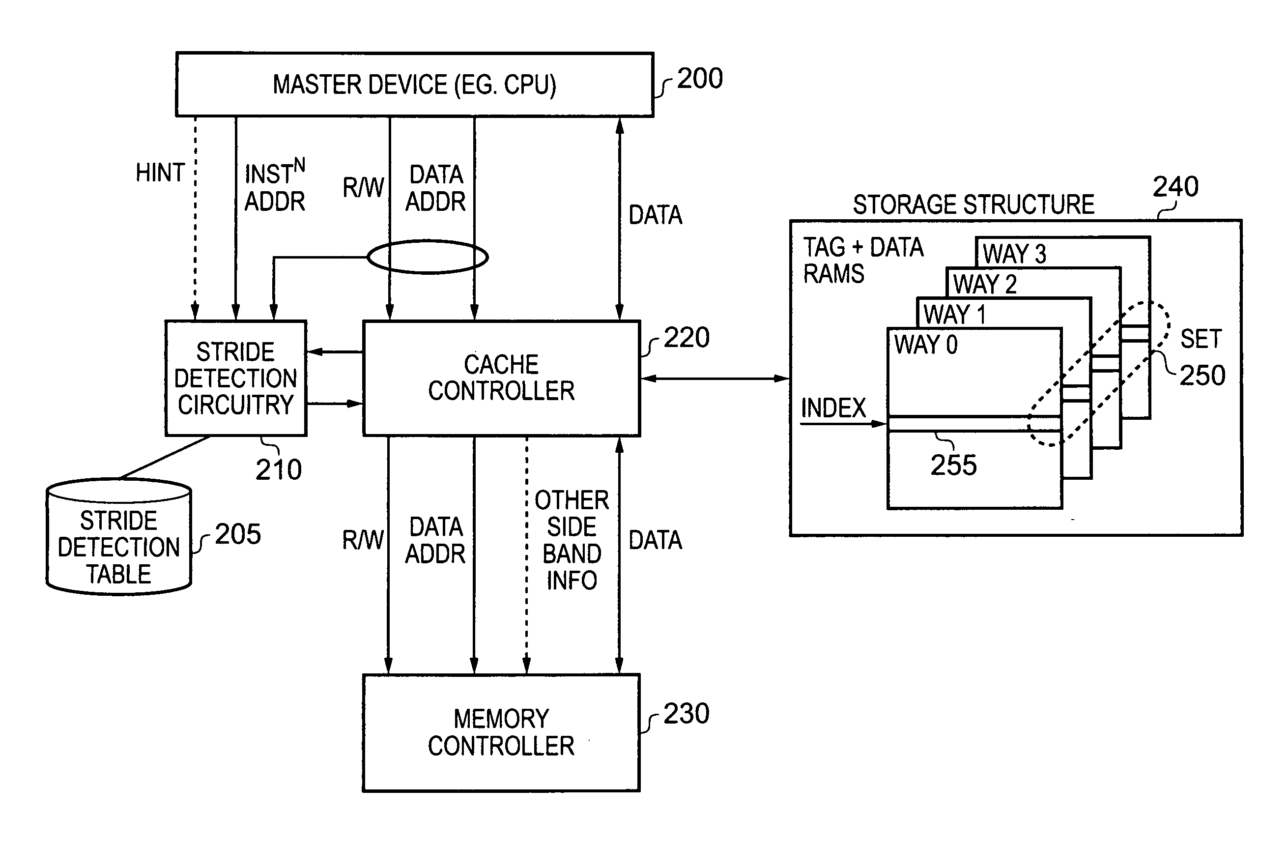
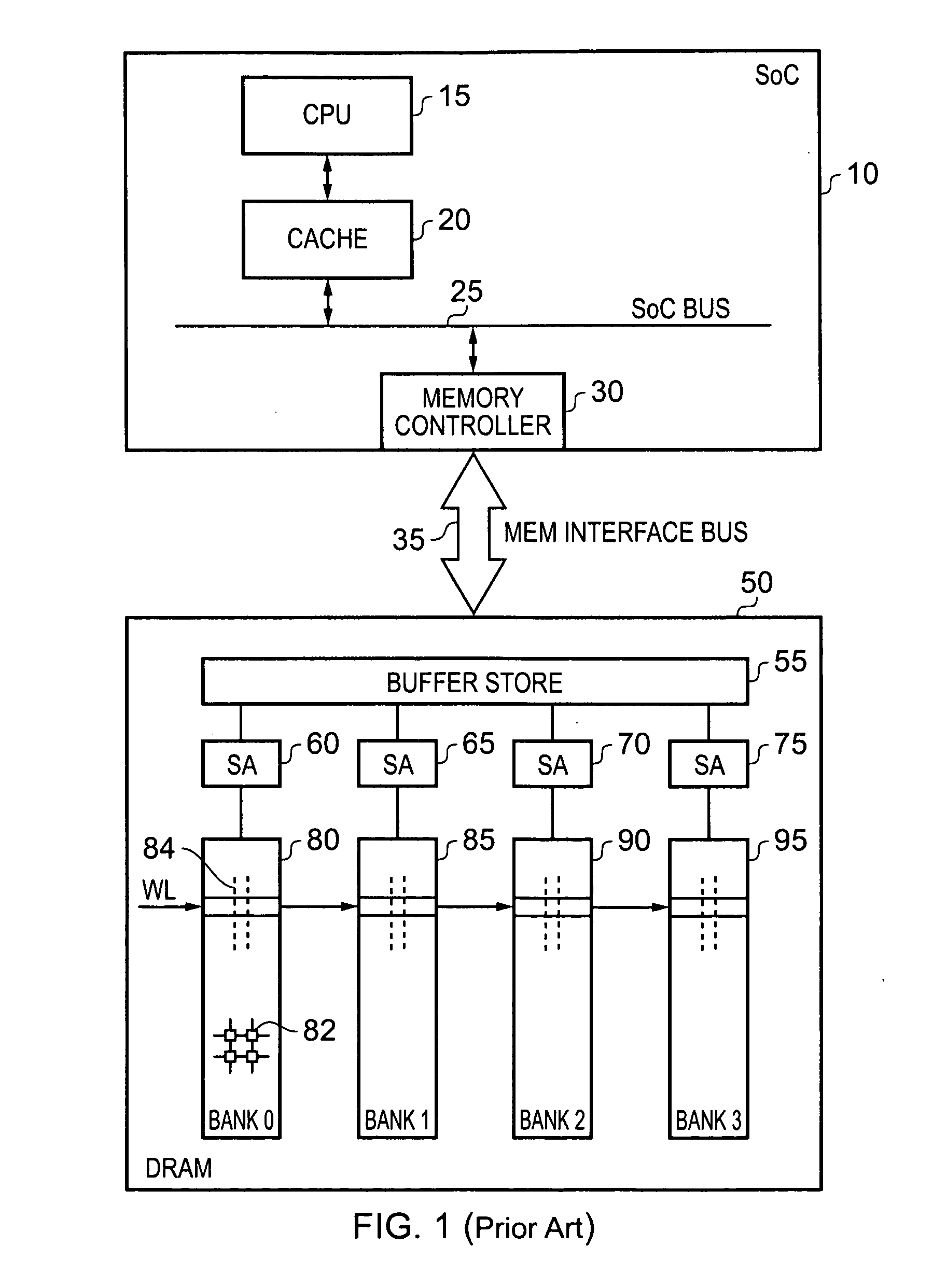
[0082]FIG. 4A is a block diagram illustrating a data processing apparatus in accordance with one embodiment. The various elements shown in FIG. 4A may in one embodiment reside within a SoC, with the memory controller 230 providing an interface from the SoC to a memory, in one embodiment the memory being a DRAM such as the DRAM 50 shown in FIG. 1. As shown in FIG. 4A, a master device 200, for example a CPU, is coupled with the memory controller 230 via a cache structure consisting of a cache controller 220 and the storage structure of the cache 240. In one embodiment, the storage structure 240 takes the form of an n-way set associative storage structure, in the particular example illustrated the storage structure being a four-way set associative storage structure. Typically, tag and data RAMS will be provided for each way, and when the master device 200 issues a request for data, a portion of the data address output by the master device will be used to derive an index into the cache....


PUM


Abstract

A cache device is provided for use in a data processing apparatus to store data values for access by an associated master device. Each data value has an associated memory location in a memory device, and the memory device is arranged as a plurality of blocks of memory locations, with each block having to be activated before any data value stored in that block can be accessed. The cache device comprises regular access detection circuitry for detecting occurrence of a sequence of accesses to data values whose associated memory locations follow a regular pattern. Upon detection of such an occurrence of a sequence of accesses by the regular access detection circuitry, an allocation policy employed by the cache to determine a selected cache line into which to store a data value is altered with the aim of increasing a likelihood that when an evicted data value output by the cache is subsequently written to the memory device, the associated memory location resides within an already activated block of memory locations. Hence, by detecting regular access patterns, and altering the allocation policy on detection of such patterns, this enables a reuse of already activated blocks within the memory device, thereby significantly improving memory utilisation, thereby giving rise to both performance improvements and power consumption reductions.

Description

BACKGROUND OF THE INVENTION[0001]1. Field of the Invention[0002]The present invention relates to a cache device for coupling to a memory device, and to a method of operation of such a cache device. In particular the present invention relates to a cache device for coupling to a memory device arranged as a plurality of blocks of memory locations, where each block has to be activated before any data value stored in that block can be accessed.[0003]2. Description of the Prior Art[0004]Many system memories (including, for example, DRAM) feature a property where sequential accesses are processed faster than non-sequential accesses. Many system memories (especially DRAM) also have the concept of page access, where access to a previously opened page is faster than to one that has never been accessed. Further, memories typically have a limit on the number of pages being open at one time, having to close a page in order to open a new one.[0005]For performance and energy consumption reasons, i...

Claims


Application Information

Patent Timeline
Patent Type & Authority Applications(United States)
IPC IPC(8): G06F12/08G06F12/00
CPCY02B60/1225G06F12/121G06F12/0895Y02D10/00
Inventor PAVER, NIGEL CHARLESBILES, STUART DAVIDSUNWOO, DAMRAMRAKHYANI, PRAKASH SHYAMLAL
Owner ARM LTD
Why Eureka
Try Eureka