Semiconductor memory and method for operating the semiconductor memory

a technology of semiconductor memory and semiconductor chips, applied in the field of semiconductor memory, can solve the problem that the chip size of the semiconductor memory may become larger

Active Publication Date: 2011-12-29
FUJITSU SEMICON MEMORY SOLUTION LTD
View PDF3 Cites 15 Cited by
  • Summary
  • Abstract
  • Description
  • Claims
  • Application Information

AI Technical Summary

Problems solved by technology

As a result, a scale of the logic circuit to select the plate lines may become la

Method used


Image

  • Semiconductor memory and method for operating the semiconductor memory
  • Semiconductor memory and method for operating the semiconductor memory
  • Semiconductor memory and method for operating the semiconductor memory

Examples


Embodiment Construction

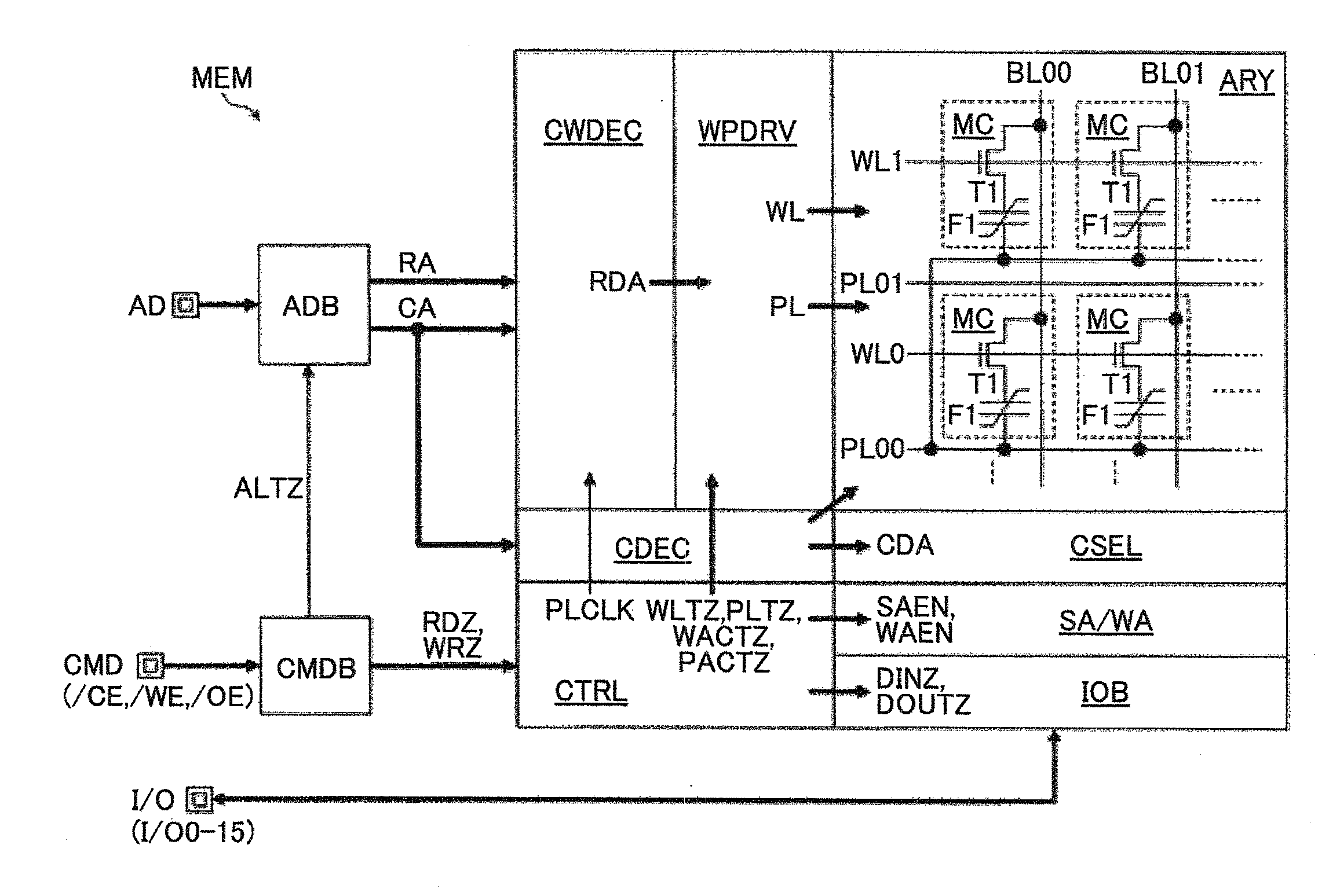
In the following, embodiments are described with reference to the accompanying drawings. In the figures, a signal line illustrated by a bold line represents plural lines unless otherwise described. Further, a part of a block to which the bold line is coupled represents plural circuits. For a signal line transmitting a signal, the same symbol as the signal name is used. A signal having “Z” as a suffix indicates positive logic. A signal having “ / ” as a header indicates negative logic. A double-square symbol in the figures presents an external terminal. The external terminal includes a pad on a semiconductor chip, a lead wire of a package containing the semiconductor chip and the like. Regarding a signal supplied through the external terminal, the same symbol as the terminal name is used.

FIG. 1 illustrates a semiconductor memory MEM according to an embodiment. For example, the semiconductor memory MEM may be formed as a ferroelectric memory on a silicon substrate using a CMOS (Compleme...


PUM


Abstract

A semiconductor memory includes memory cells; word lines coupled to the memory cells; plate lines coupled to the memory cells; a selector that selects a first address signal in a first period and select a second address ,signal in a second period; a decode circuit that sequentially decodes the first and the second address signals selected by the selector, sequentially generates decode address signals based on the decoded first and second address signals, and sequentially activates the generated decode address signals; and a driver circuit that drives the word lines in accordance with the decode address signals activated based on the first address signal and drives the plate lines in accordance with the decode address signals activated based on the second address signal.

Description

FIELDThe embodiment discussed herein is related to a semiconductor memory including word lines and plate lines wired in memory cells.BACKGROUNDIn a semiconductor memory such a ferroelectric memory, a plate line is commonly coupled to ferroelectric capacitors in plural memory cells, and the load capacity of the plate line is large. Because of those features, a waveform of a signal transmitted in the plate line may be rounded and a drive time using such a plate line may become longer. As a result, access time of the memory cell may be extended. To reduce the load capacity of the plate line, there is a known method of dividing the plate line into plural plate-line segments to reduce the number of memory cells coupled to each of the divided plural plate-line segments (see, for example, Japanese Laid-open Patent Publication No. 10-229171).However, when the plate line is divided as such, the number of plate lines is accordingly increased. As a result, a scale of the logic circuit to selec...

Claims


Application Information

Patent Timeline
IPC IPC(8): G11C8/08G11C8/10
CPCG11C8/08G11C11/22G11C8/10
Inventor NAKAZAWA, MITSUHARU
Owner FUJITSU SEMICON MEMORY SOLUTION LTD
Why Eureka
Try Eureka