Semiconductor structure and method of fabricating the same

a semiconductor and circuit technology, applied in semiconductor/solid-state device manufacturing, basic electric elements, electric instruments, etc., can solve the problems of laterally oriented devices consuming significant chip area, complex and expensive to fabricate a computer chip with memory embedded in this way, and the masks used to fabricate memory devices are generally not compatible with the masks used

Inactive Publication Date: 2012-01-05
BESANG
View PDF2 Cites 228 Cited by
  • Summary
  • Abstract
  • Description
  • Claims
  • Application Information

AI Technical Summary

Problems solved by technology

However, these laterally oriented devices consume significant amounts of chip area.
However, there are several problems with doing this.
One problem is that the masks used to fabricate the memory devices are generally not compatible with the masks used to fabricate the other devices on the computer chip.
Hence, it is more complex and expensive to fabricate a computer chip with memory embedded in this way.
Another problem is that memory devices tend to be large and occupy a significant amount of area.
Further, the yield of the computer chips fabricated in a run decreases as their area increases, which increases the overall cost.
There are several problems, however, with using 3-D packages and 3-D ICs.
One problem is that the use of wire bonds increases the access time between the computer and memory chips because the impedance of wire bonds and large contact pads is high.
Similarly, the contact pads in 3-D ICs have correspondin

Method used


Image

  • Semiconductor structure and method of fabricating the same
  • Semiconductor structure and method of fabricating the same
  • Semiconductor structure and method of fabricating the same

Examples


Embodiment Construction

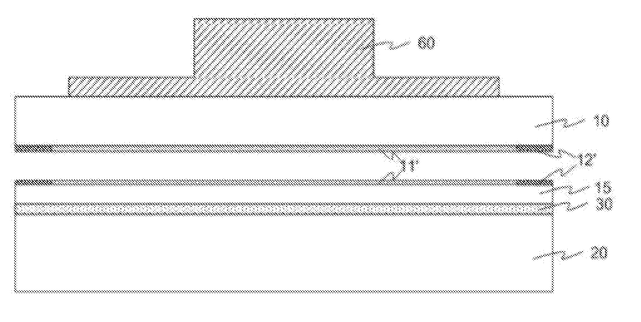
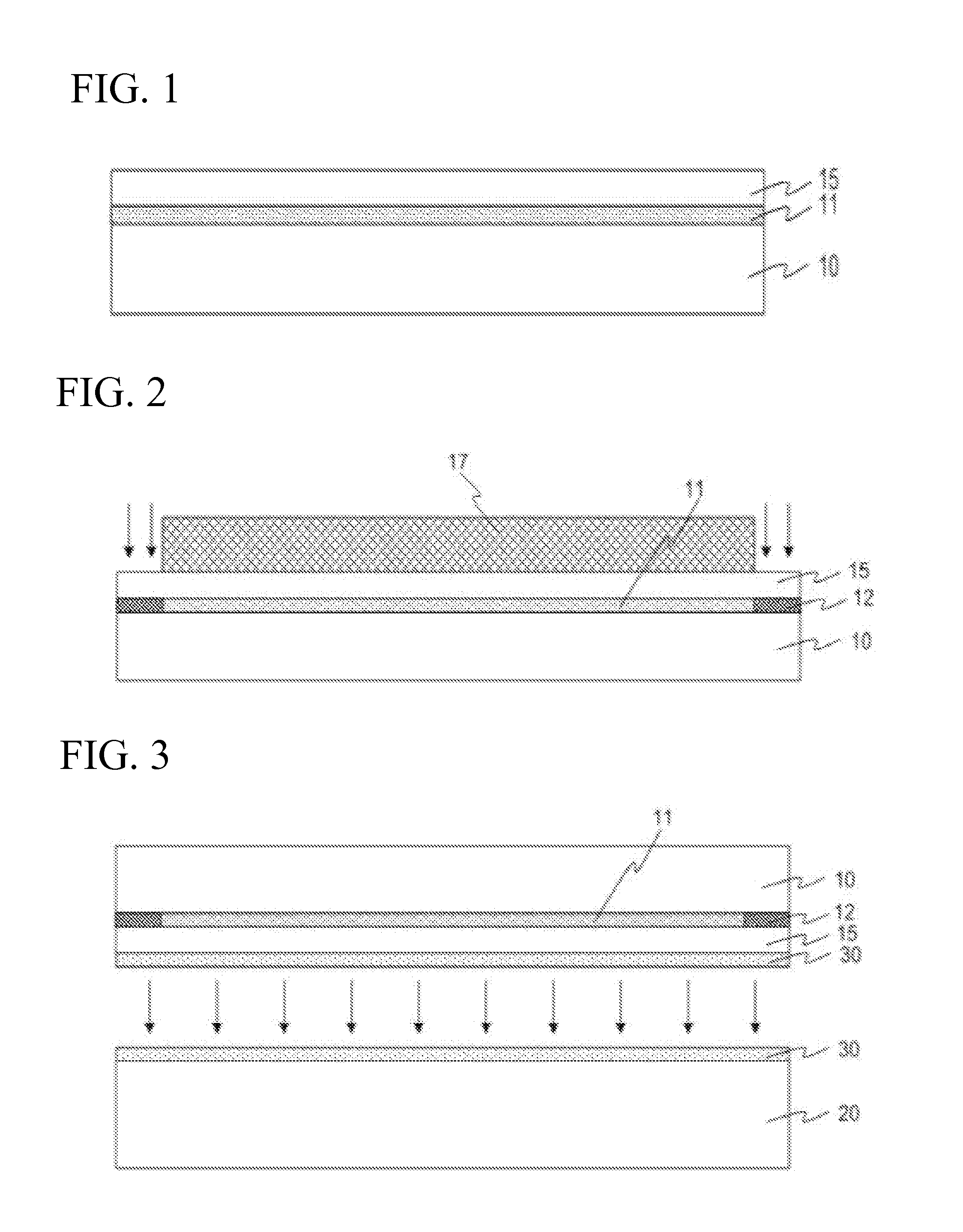
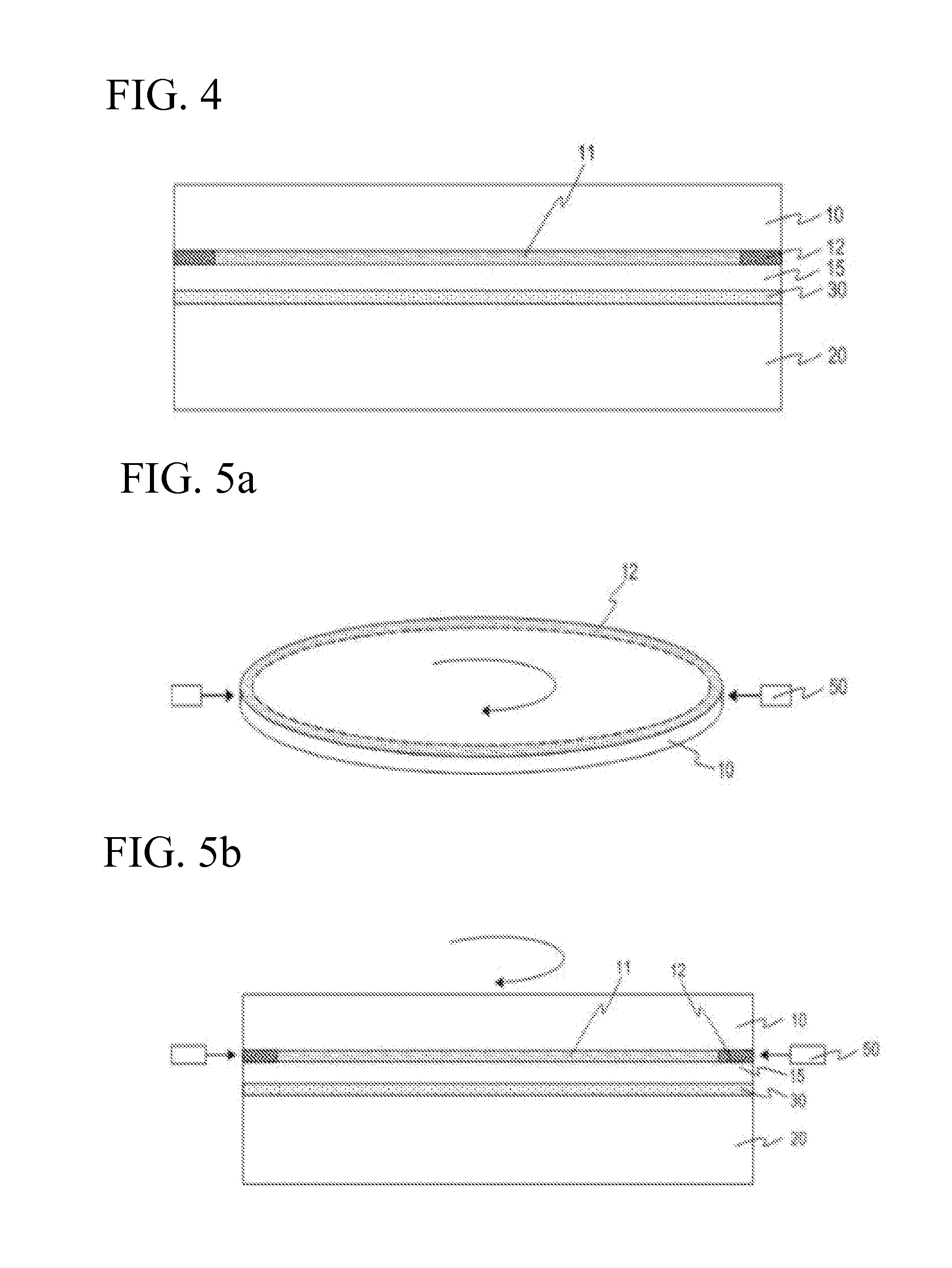
[0018]A method for fabricating a semiconductor substrate and a method for fabricating a semiconductor device by using the same, more specifically relates to a method for fabricating a semiconductor substrate and a method for fabricating a semiconductor device by using the same more reliable and repeatable is provided. The method is comprised of, providing a first semiconductor substrate including a detaching layer in a pre-defined depth from the surface; forming ion-implanted layer around edge of the detaching layer; bonding a second semiconductor substrate to the first semiconductor substrate; forming crack in the ion-implanted layer by adding stress to the ion-implanted layer; and detaching portion of the first semiconductor substrate by spreading out the crack from the ion-implanted layer through the detaching layer, and also the method is comprised of providing a first semiconductor substrate including a detaching layer in a pre-defined depth from the surface; forming ion-implan...


PUM


Abstract

A method of fabricating a semiconductor substrate includes providing a first semiconductor substrate, which includes a detaching layer spaced from an upper surface of the first semiconductor substrate; forming an ion-implanted layer proximate to an edge of the detaching layer; bonding a second semiconductor substrate to the first semiconductor substrate; forming a crack in the ion-implanted layer in response to applying stress to the ion-implanted layer; and detaching a portion of the first semiconductor substrate in response to cleaving through the crack.

Description

CROSS-REFERENCE TO RELATED APPLICATIONS[0001]This patent application claims priority to Korean Patent Application No. 10-2009-63943, which was filed on Jul. 2, 2010, by the same inventor, the contents of which are incorporated by reference as though fully set forth herein.BACKGROUND OF THE INVENTION[0002]1. Field of the Invention[0003]This invention relates to semiconductor circuitry formed using bonding.[0004]2. Description of the Related Art[0005]Advances in semiconductor manufacturing technology have provided computer systems with integrated circuits that include many millions of active and passive electronic devices, along with the interconnects to provide the desired circuit connections. A typical computer system includes a computer chip, with processor and control circuits, and an external memory chip. As is well-known, most integrated circuits include laterally oriented active and passive electronic devices that are carried on a single major surface of a substrate. The curren...

Claims


Application Information

Patent Timeline
IPC IPC(8): H01L21/304
CPCH01L21/268H01L21/76259H01L21/76254H01L21/304
Inventor LEE, SANG-YUN
Owner BESANG
Why Eureka
Try Eureka