Microelectronic packages with dual or multiple-etched flip-chip connectors

a technology of flip-chip connectors and microelectronic packages, which is applied in the direction of electrical equipment, semiconductor devices, semiconductor/solid-state device details, etc., can solve the problems of difficult or impossible to form arrays of microcontacts with appreciable height, very small pitch or spacing, and limited configuration of microcontacts formed by conventional etching processes

Active Publication Date: 2012-01-12
TESSERA INC
View PDF6 Cites 116 Cited by
  • Summary
  • Abstract
  • Description
  • Claims
  • Application Information

AI Technical Summary

Problems solved by technology

It has been difficult or impossible to form arrays of microcontacts with appreciable height and very small pitch or spacing betwe

Method used


Image

  • Microelectronic packages with dual or multiple-etched flip-chip connectors
  • Microelectronic packages with dual or multiple-etched flip-chip connectors
  • Microelectronic packages with dual or multiple-etched flip-chip connectors

Examples


Embodiment Construction

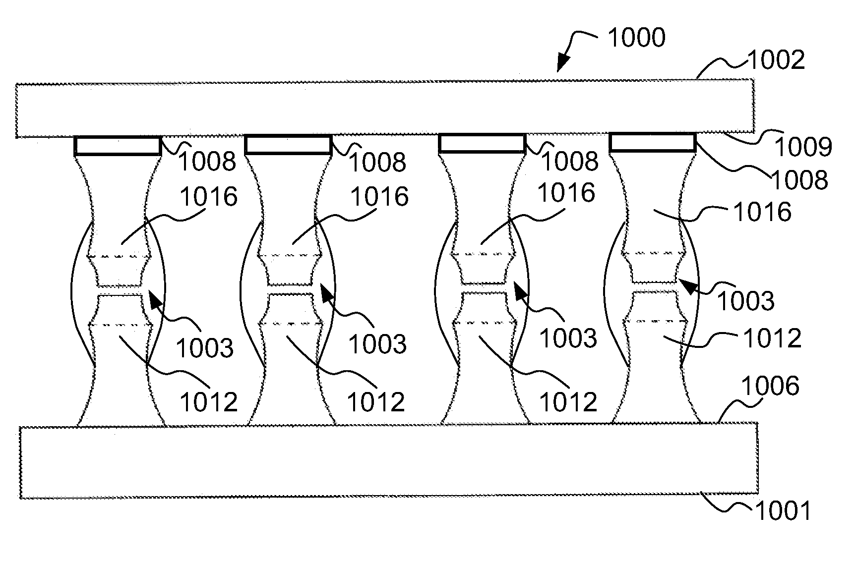
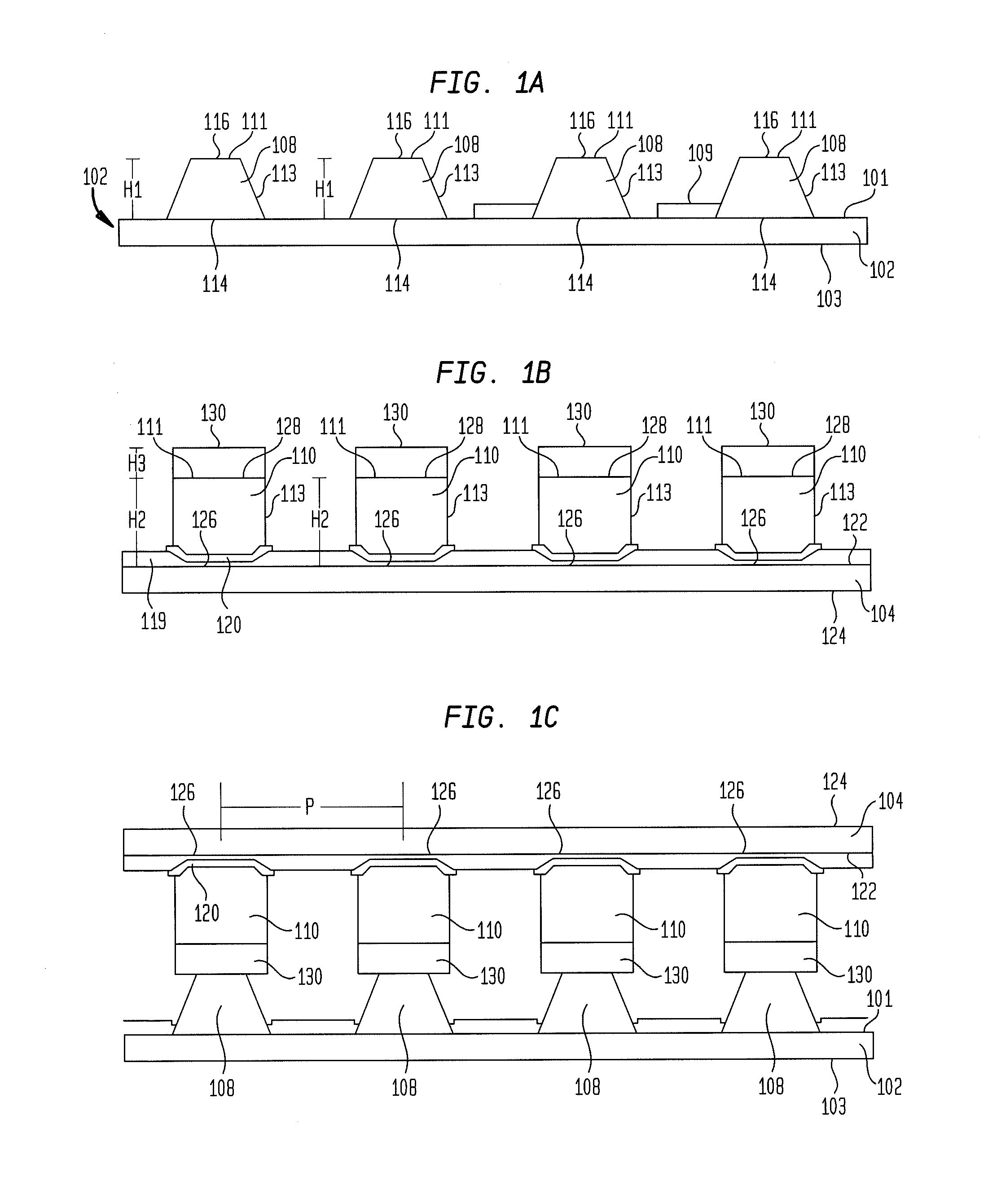
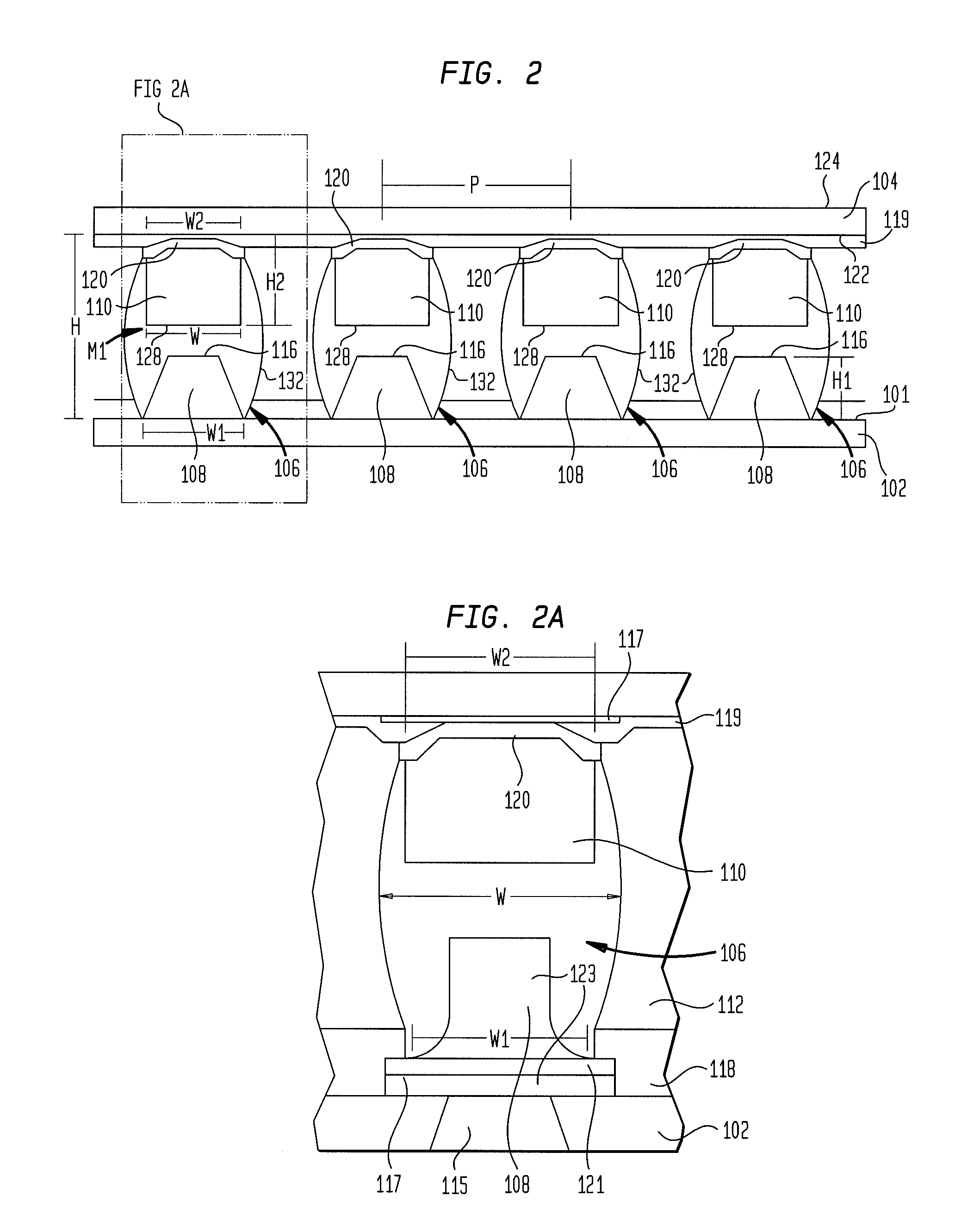
[0058]Reference is now made to FIGS. 1A-1C, which illustrate cross-sectional views of the components of the packaged microelectronic assembly 100 shown in FIG. 2. As shown, the packaged microelectronic assembly 100 includes a substrate 102, a microelectronic element 104 in a face down or flip-chip position, and conductive columns 106 joining the substrate with the microelectronic element. The conductive columns include conductive bumps or posts 108 which protrude above a face 105 of the substrate 102 that are aligned with conductive bumps or posts 110 protruding above a face 107 of the microelectronic element 104. The conductive columns 106 provide for increased height for chip-on-substrate packaging by increasing the standoff or vertical distance between the microelectronic element 104 and substrate 102, while at the same time allowing for a decrease in the center-to-center horizontal distance or pitch P between conductive columns 106. As will be discussed in further detail below, ...


PUM


Abstract

A packaged microelectronic element includes a microelectronic element having a front surface and a plurality of first solid metal posts extending away from the front surface. A substrate has a major surface and a plurality of conductive elements exposed at the major surface and joined to the first solid metal posts. In particular examples, the conductive elements can be bond pads or can be second posts having top surfaces and edge surfaces extending at substantial angles away therefrom. Each first solid metal post includes a base region adjacent the microelectronic element and a tip region remote from the microelectronic element, the base region and tip region having respective concave circumferential surfaces. Each first solid metal post has a horizontal dimension which is a first function of vertical location in the base region and which is a second function of vertical location in the tip region.

Description

BACKGROUND OF THE INVENTION[0001]The present invention relates to microelectronic packages, to components for use in fabrication of microelectronic packages, and to methods of making the packages and components.[0002]Microelectronic devices generally comprise a thin slab of a semiconductor material, such as silicon or gallium arsenide, commonly called a die or a semiconductor chip. Semiconductor chips are commonly provided as individual, prepackaged units. In some unit designs, the semiconductor chip is mounted to a substrate or chip carrier, which is in turn mounted on a circuit panel, such as a printed circuit board.[0003]In one face of the semiconductor chip is fabricated the active circuitry. To facilitate electrical connection to the active circuitry, the chip is provided with bond pads on the same face. The bond pads are typically placed in a regular array either around the edges of the die or, for many memory devices, in the die center. The bond pads are generally made of a c...

Claims


Application Information

Patent Timeline
IPC IPC(8): H01L23/498H01L21/60
CPCH01L2224/11472H01L2224/13018H01L2224/116H01L2224/17515H01L2225/06517H01L2924/10329H01L2225/0652H01L2924/01078H01L2224/81193H01L2924/01032H01L2224/81893H01L2924/01022H01L21/563H01L2924/01057H01L2224/114H01L21/4853H01L24/11H01L2224/16238H01L2924/01029H01L2224/13144H01L2924/01019H01L2924/10253H01L2224/81203H01L23/49827H01L2924/0105H01L2224/81805H01L23/49811H01L24/05H01L2924/01024H01L2924/01322H01L2924/00013H01L24/81H01L2224/16225H01L2224/05644H01L2924/01079H01L24/16H01L23/48H01L2224/0401H01L2224/16227H01L2224/0558H01L2224/13082H01L2224/8182H01L2924/01033H01L2224/13147H01L2224/13021H01L2924/014H01L2924/01013H01L24/13H01L23/49822H01L2224/81815H01L25/105H01L2924/01005H01L2924/01074H01L2224/814H01L2924/01006H01L2224/13017H01L23/49816H01L2224/11901H01L2224/81136H01L2224/0612H01L2924/00014H01L2224/13099H01L2924/00H01L2924/00012H01L23/481
Inventor HABA, BELGACEM
Owner TESSERA INC
Why Eureka
Try Eureka