2d coil and a method of obtaining ec response of 3D coils using the 2d coil configuration

a technology of 2d coils and configurations, applied in the direction of magnetic properties, instruments, material magnetic variables, etc., can solve the problems of insensitive arrangements, inability to overcome conductivity and permeability changes, and difficulty, etc., to achieve the effect of reducing costs, facilitating access, and high resolution

Active Publication Date: 2012-01-12
OLYMPUS NDT
View PDF0 Cites 19 Cited by
  • Summary
  • Abstract
  • Description
  • Claims
  • Application Information

AI Technical Summary

Benefits of technology

[0025]The method herein disclosed makes it possible to use 2D wound EC sensors to obtain defect signatures in the impedance plane very similar to, if not identical with, those obtained from their conventional 3D counterparts.
[0026]The significant benefit of the herein disclosed 2D sensor includes largely reducing the cost associated with manufacturing when using the 2D wound EC sensor to replace its 3D counterpart.
[0027]Other advantages inherently provided by the herein disclosed 2D wound EC sensors include being able to fabricate using PCB technologies, manufacturing with a fully automated process as compared to manually for its 3D counterpart, and having sensors that are very thin, mechanically flexible, if necessary, and easy to be used to access tight spaces for inspection.
[0028]Another advantage of the herein disclosed 2D EC sensor is that it allows the configuration of adding plurality of layers of such sensors to provide scanning with higher resolution.
[0029]Yet another advantage of the disclosed 2D sensor is that superior coupling is obtained between the herein disclosed sensor and the test surface which provides an increased signal strength.

Problems solved by technology

In such prior systems, difficulties are encountered due to the changes in conductivity and permeability of the part under test and also due to the variations in spacing between the test coil or probe and the surface of the part, and variation in surface conditions.
Such arrangements, however, have not overcome the sensitivity to conductivity and permeability changes.
However, such arrangements have been insensitive to defects common to the differentially connected coils.
The 3D orthogonal sensor topology described above provides many benefits; however, a few drawbacks have been known to bring limitations to its usage.
One such drawback is that, with coils wound onto a cube or cross-shaped core, the sensor is inevitably bulky, which limits the space it can access during inspections.
Another drawback is that the fabrication of this sensor largely depends on having the coils manually wound onto the cubes or the cross-shaped cores.
The fabrication is labor intensive and costly.
A drawback of currently available EC sensors or probes made from printed circuit boards is that they are limited to simply mapping the two-dimensional (2D) shape of the prior art coils that are wound on a plane that is approximately parallel to the inspected surface.
However, challenges remain in PCB manufacturing for some coil configurations such as used in the orthogonal sensors with a 3D structure.
While this technology benefits some applications, it is unable to provide a fully flexible probe because the AMR and GMR sensors are discrete components on the PCB.
There are also many limitations intrinsic to AMR and GMR sensors such as the risk of saturation and the need for magnetic biasing, both of which presents undesirable concerns in an industrial environment.

Method used


Image

  • 2d coil and a method of obtaining ec response of 3D coils using the 2d coil configuration
  • 2d coil and a method of obtaining ec response of 3D coils using the 2d coil configuration
  • 2d coil and a method of obtaining ec response of 3D coils using the 2d coil configuration

Examples


Embodiment Construction

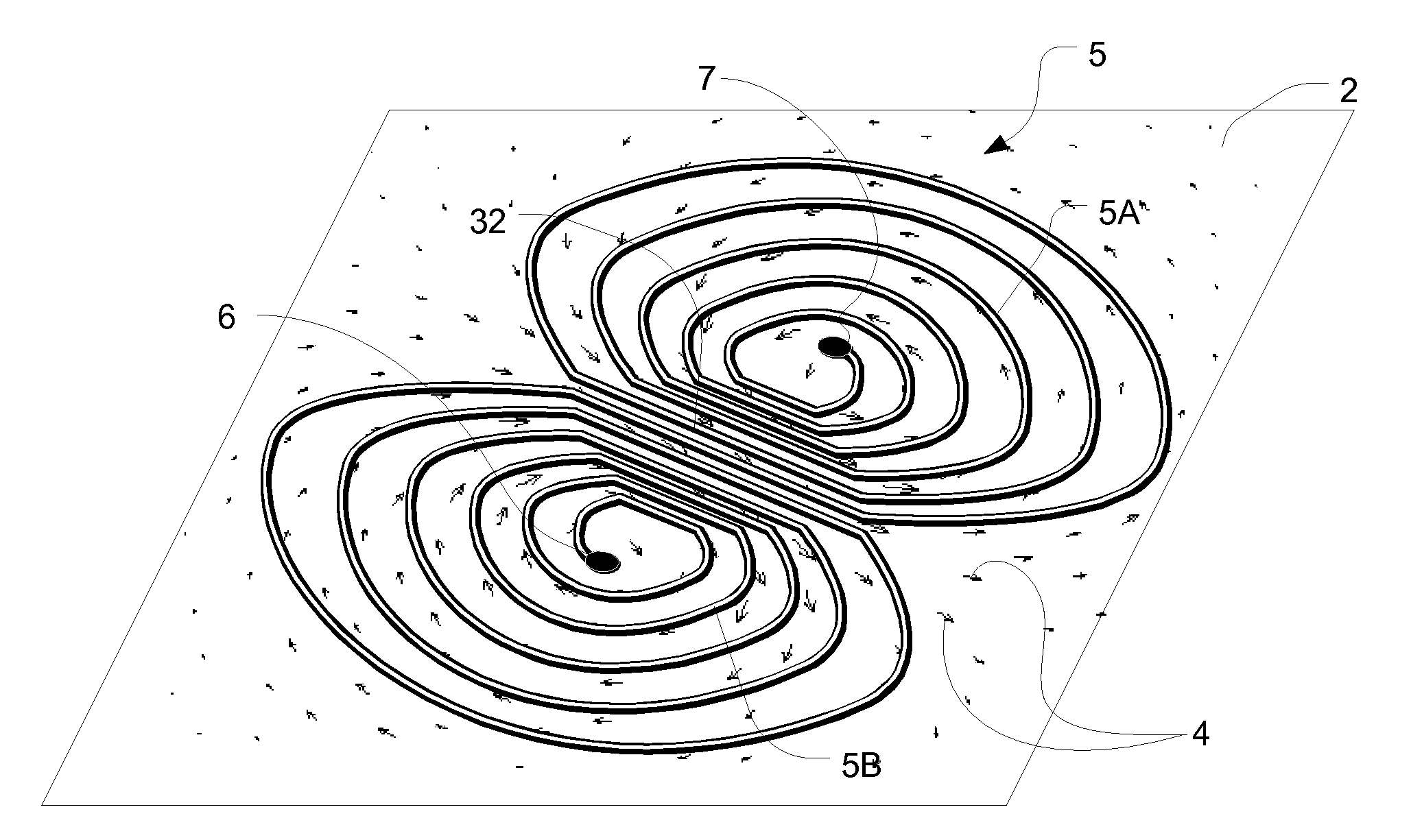
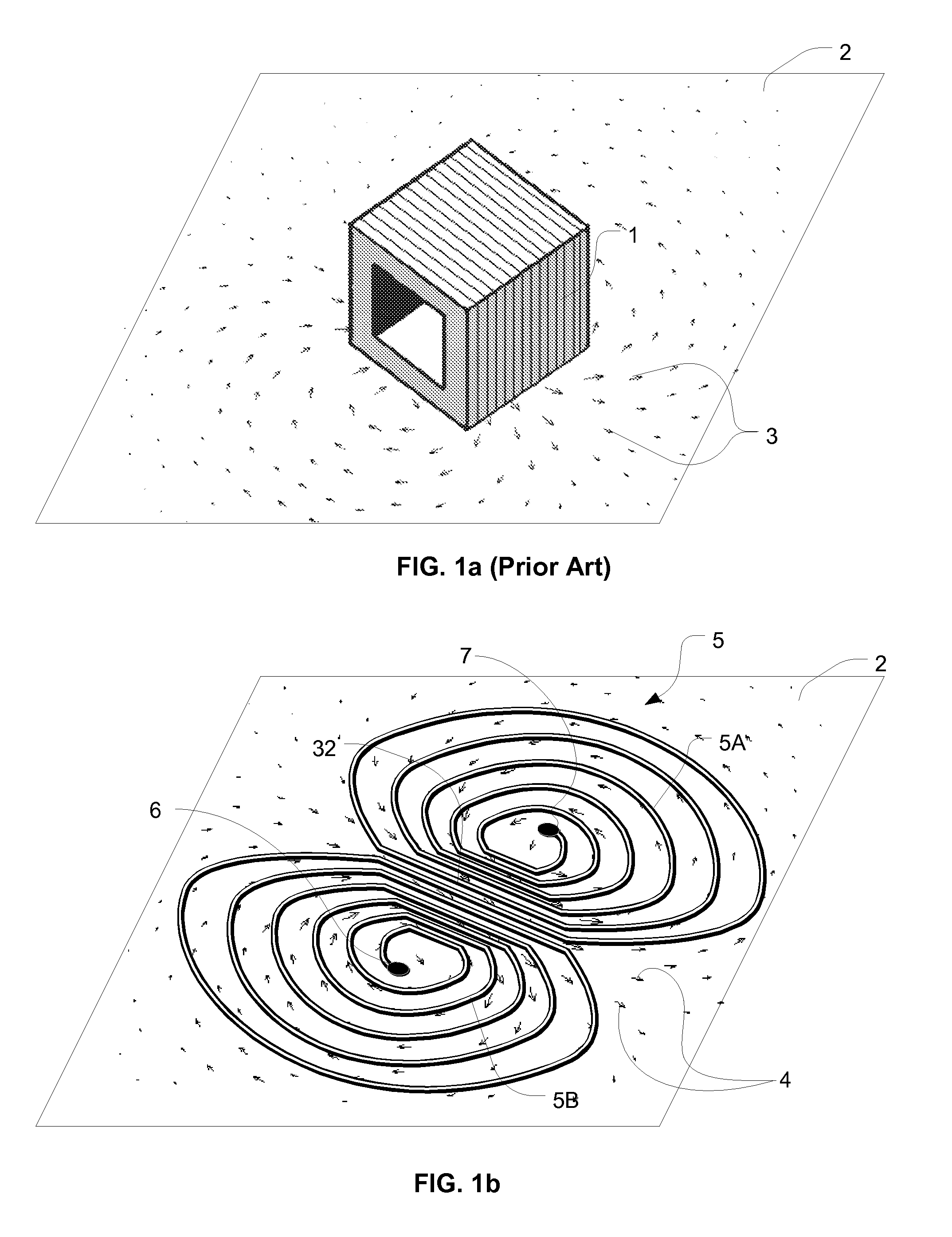
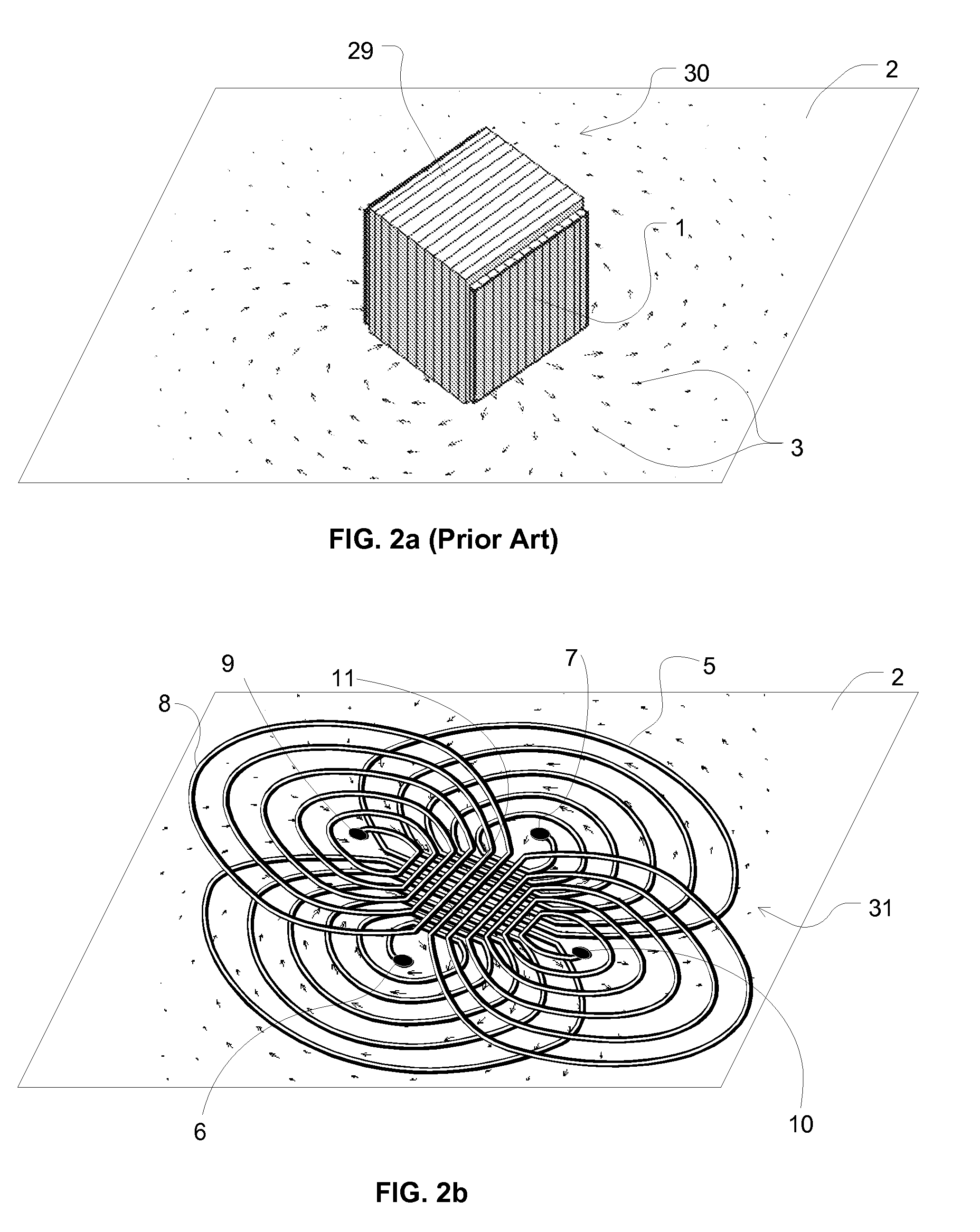
[0036]FIG. 1a shows an EC flow 3 induced on a conductive test surface 2 by a conventional 3D EC drive coil 1. As can be seen, the driver coil 1 is wound on a 3D cubic core and the winding path includes two planes perpendicular to surface 2. In general, if EC drivers are wound on a winding plane parallel to the test surface, the induced EC flow on the test surface is parallel to the driver coil. For the case of the 3D EC drive, drive coil 1 is wound on a 3D structure that contains planes that are erected from (not parallel to) the test surface, whereas EC flow 3 is confined within test surface 2. EC flow 3 can therefore not always be parallel to driver coil 1. Instead, EC flow 3 is driven by the interaction between surface 2 and the magnetic flow generated by the driver 1 at surface 2 and forms a pair of whirls on surface 2 as shown in FIG. 1a.

[0037]Referring now to FIG. 1b, a basic embodiment of the present disclosure is shown to include a pair of whirl-shaped 2D coil wound on a pl...


PUM


Abstract

The invention herein disclosed provides a 2D coil and a method of using the 2D wound EC sensor for reproducing the Eddy Current Testing (ECT) response of a prior art 3D orthogonal sensor. The 3D orthogonal sensor is conventionally wound onto a 3D core, with at least some of the surfaces being un-parallel to the surface be inspected. Using the herein disclosed 2D configuration allows the use of printed circuit board technologies for the manufacturing of these EC sensors. The herein disclosed method and the associated 2D EC sensors are particularly useful for reproducing the EC effect of conventional orthogonal probe arrays.

Description

FIELD OF THE INVENTION[0001]The present invention relates to non-destructive testing and inspection systems (NDT / NDI), particularly to a method of emulating eddy current (EC) fields generated by a 3D coil using a 2D coil configuration which can be fabricated on a printed circuit board (PCB).BACKGROUND OF THE INVENTION[0002]EC inspection is commonly used in NDT / NDI applications to detect flaws in surfaces of manufactured components fabricated out of conductive materials, such as steel bars, tubes and pipes. EC is often used to inspect components for automotive, aeronautic and energy industries. Over the years, EC sensors have been designed with different configurations and patterns to suit for different applications.[0003]Various EC systems have heretofore been provided for the detection of cracks and or other flaws in a part under test. In general, such systems include field producing means such as a coil connected to an AC source to generate EC's in a part and a sensing means to se...

Claims


Application Information

Patent Timeline
Patent Type & Authority Applications(United States)
IPC IPC(8): G01R33/12
CPCG01N27/904G01N27/9006
Inventor LEPAGE, BENOIT
Owner OLYMPUS NDT
Why Eureka
Try Eureka