Monolithic microwave integrated circuit

a monolithic, integrated circuit technology, applied in the direction of basic electric elements, transistors, inductances, etc., can solve the problems that the conventional approach of monolithic forming such active and passive elements on a common substrate has not proved practical for microwave structures

Active Publication Date: 2012-02-16
NXP USA INC
View PDF59 Cites 60 Cited by
  • Summary
  • Abstract
  • Description
  • Claims
  • Application Information

AI Technical Summary

Problems solved by technology

However, as the desired operating frequencies have increased, conventional approaches for monolithically forming such active and passive elements on a common subs...

Method used


Image

  • Monolithic microwave integrated circuit
  • Monolithic microwave integrated circuit
  • Monolithic microwave integrated circuit

Examples


first embodiment

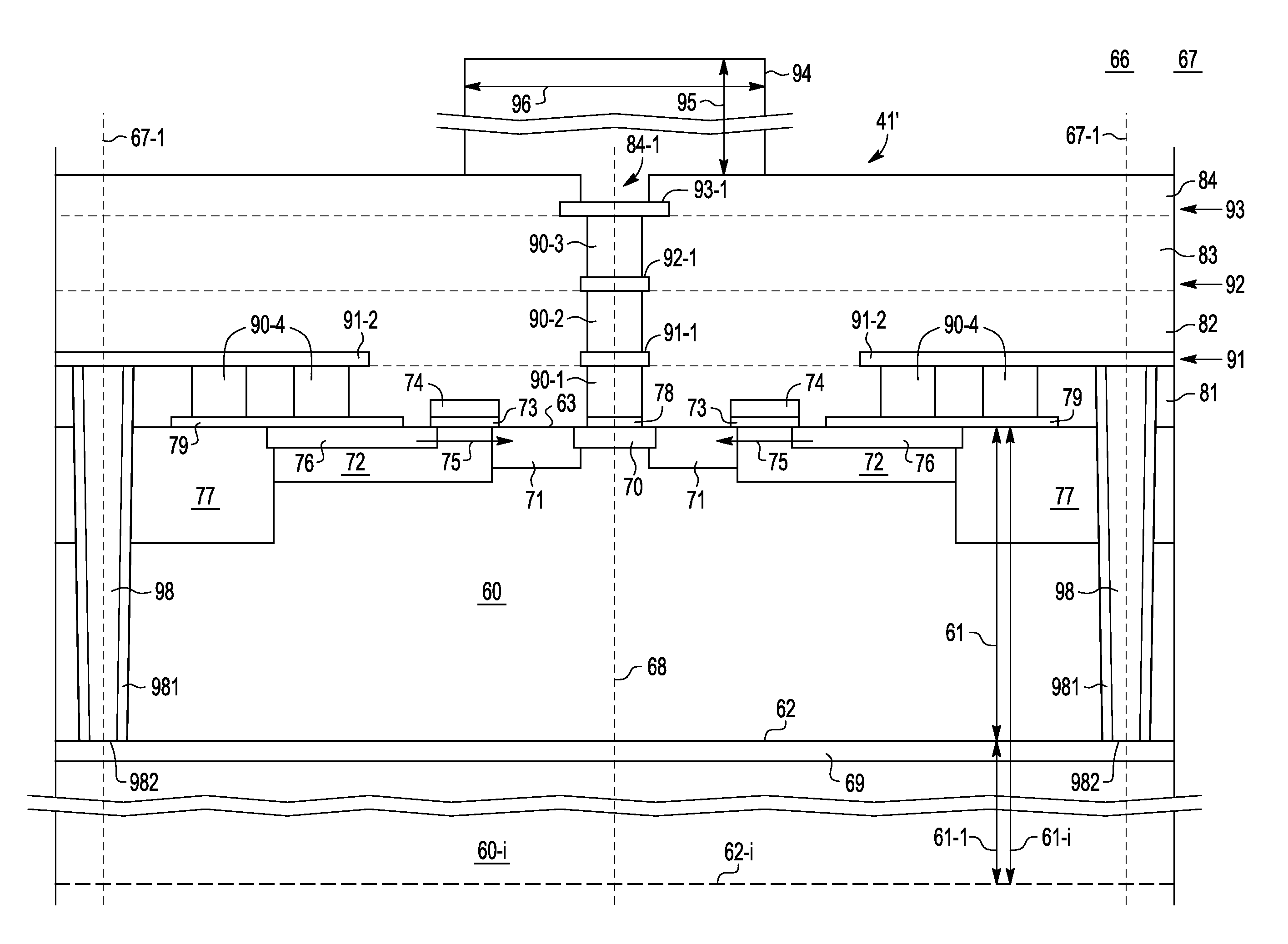
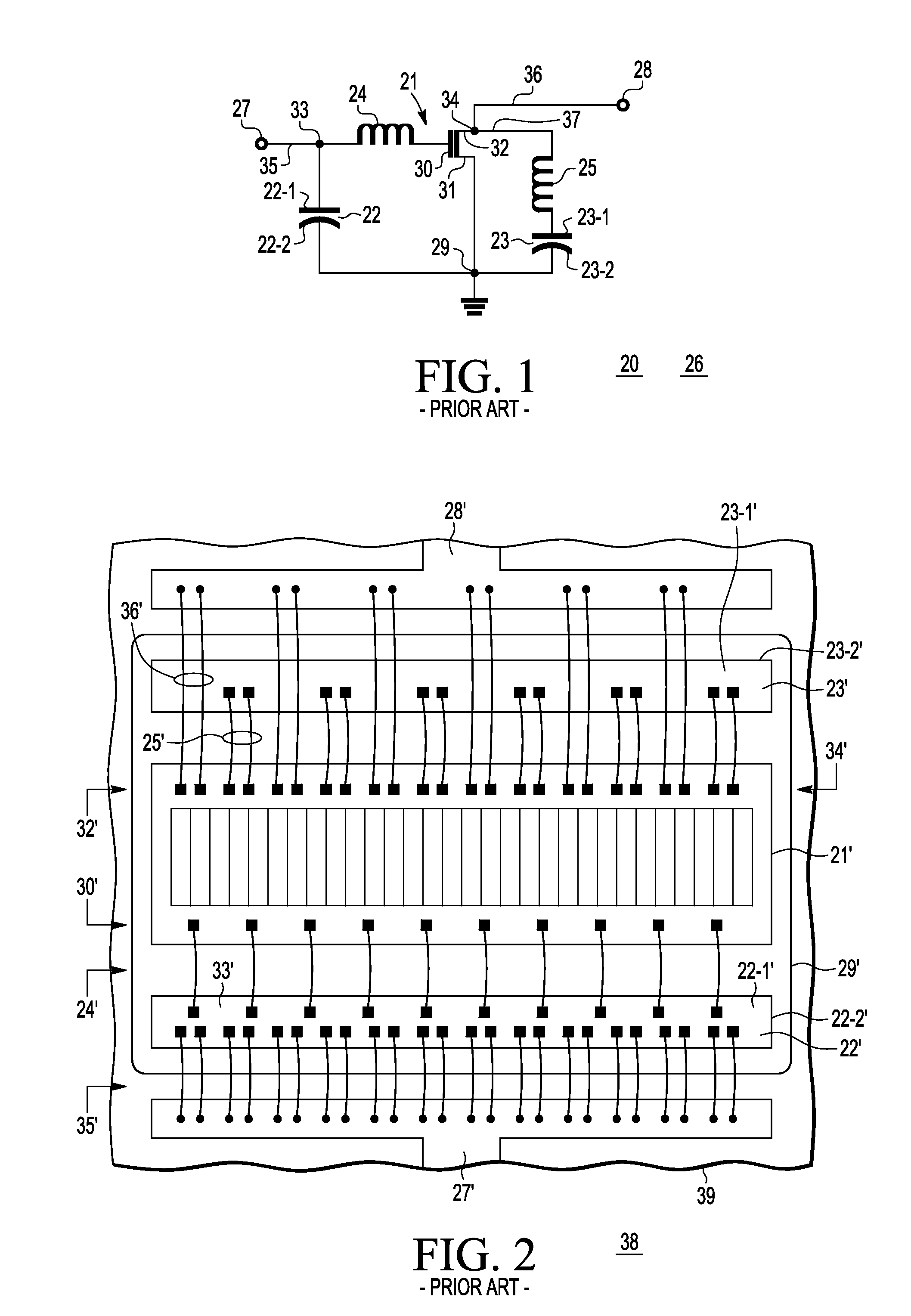
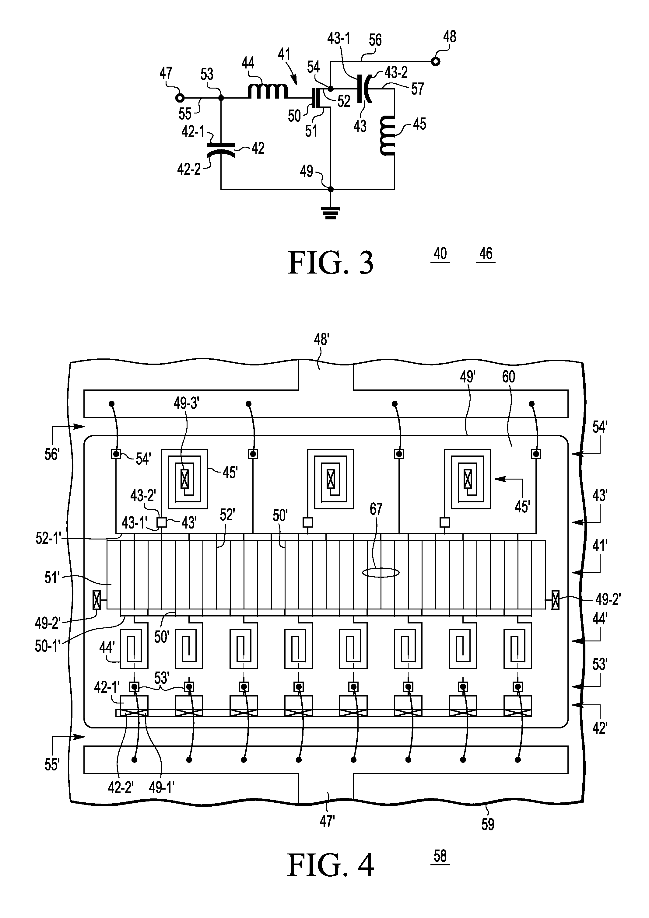
[0039] there is provided a monolithic microwave integrated circuit (46, 58), comprising, a semiconductor substrate (60) having a bulk resistivity equal or greater than about 100 Ohm-cm, and having a front surface (63) and a rear surface (62), at least one transistor (41) formed in the semiconductor substrate (60) and having an input terminal (50), an output terminal (52) and a reference terminal (51), at least one capacitor (42′, 43′) monolithically formed over the semiconductor substrate (60), at least one inductor (44′, 45′) monolithically formed over the semiconductor substrate (60), and planar interconnections overlying the semiconductor substrate (60) coupling the at least one transistor (41′), capacitor (42′, 43′), and inductor (44′, 45′) to form the monolithic integrated circuit (46, 58). According to a further embodiment, the monolithic microwave integrated circuit (46, 58), further comprising an input node (53, 53′) thereof and an output node (54, 54′) thereof, both support...

second embodiment

[0040] there is provided a method for forming a monolithic microwave integrated circuit (46, 58) having an input terminal (47), an output terminal (48) and a reference terminal (49, 69, 69′), the method comprising, providing a high resistivity initial semiconductor substrate (60-i) having an initial thickness (61-i) between a first surface (63) and an initial second surface (62-i), forming at least one transistor (41′) in the initial semiconductor substrate (60-i) with input terminal (50, 50′, 74), output terminal (52, 52′, 70, 78) and reference terminal (51, 51′, 76, 79) proximate the first surface (63), forming one or more conductor filled substrate vias (49′, 98, 98′) extending into the initial semiconductor substrate (60-i) through the first surface (63), forming one or more planar capacitors (42′, 43′) over the first surface (63) of the initial substrate (60-i), each capacitor (42′, 43′) having first (42-1′, 43-1′) and second (42-2′, 43-2′) terminals, forming one or more planar...

third embodiment

[0041] there is provided a monolithic microwave integrated circuit (46, 58) having a circuit input terminal (47′), a circuit output terminal (48′) and a circuit reference terminal (49, 49′, 69, 69′), comprising, a semiconductor substrate (60) having a bulk resistivity equal or greater than about 100 Ohm-cm, and having a front surface (63) and a rear surface (62), wherein the rear surface (62) has thereon the circuit reference terminal (49, 49′, 69, 69′), at least one LDMOS transistor (41′) formed in the substrate (60) and having a transistor input terminal (50′), a transistor output terminal (52′) and a transistor reference terminal (51′), wherein the transistor reference terminal (51′) is coupled to the circuit reference terminal (49, 49′, 69, 69′), at least first (42′) and second (43′) monolithic planar capacitors overlying the front surface (63′), at least first (44′) and second (45′) monolithic planar inductors overlying the front surface (63′), and wherein the first capacitor (...


PUM


Abstract

Low Q associated with passive components of monolithic integrated circuits (ICs) when operated at microwave frequencies can be avoided or mitigated using high resistivity (e.g., ≧100 Ohm-cm) semiconductor substrates (60) and lower resistance inductors (44′, 45′) for the IC (46). This eliminates significant in-substrate electromagnetic coupling losses from planar inductors (44, 45) and interconnections (50-1′, 52-1′, 94, 94′, 94″) overlying the substrate (60). The active transistor(s) (41′) are formed in the substrate (60) proximate the front face (63). Planar capacitors (42′, 43′) are also formed over the front face (63) of the substrate (60). Various terminals (42-1′, 42-2′, 43-1, 43-2′,50′, 51′, 52′, 42-1′, 42-2′, etc.) of the transistor(s) (41′), capacitor(s) (42′, 43′) and inductor(s) (44′, 45′) are coupled to a ground plane (69) on the rear face (62) of the substrate (60) using through-substrate-vias (98, 98′) to minimize parasitic resistance. Parasitic resistance associated with the planar inductors (44′, 45′) and heavy current carrying conductors (52-1′) is minimized by placing them on the outer surface of the IC where they can be made substantially thicker and of lower resistance. The result is a monolithic microwave IC (46, 58) previously unobtainable.

Description

FIELD OF THE INVENTION[0001]The present invention generally relates to semiconductor devices and circuits and methods for fabricating semiconductor devices and circuits, and more particularly relates to monolithic integrated circuits adapted to operate at very high frequencies, including microwave frequencies.BACKGROUND OF THE INVENTION[0002]As the electronic arts have progressed there is an ongoing need for solid state circuits adapted to operate at higher and higher frequencies, including microwave frequencies. As used herein, the term “microwave” is intended to refer to frequencies at or above about 800 mega-Hertz. Various transistor structures have been created that are capable of providing gain in such frequency ranges. Passive components, e.g., inductors, and capacitors, must often be combined with such solid state amplifiers in order to achieve the desired circuit functions, for example and not intended to be limiting, power amplifiers, modulators, filters, oscillators, etc. ...

Claims


Application Information

Patent Timeline
IPC IPC(8): H01L27/06H01L21/82
CPCH01L23/481H01L27/0629H01L23/5227H01L23/66H01L27/0617H01L2223/6616H01L2223/6655H01L2223/6683H01L2924/12044H03F3/195H01L24/49H01L2224/49175H01L2924/1423H01L23/5223H01L2924/00014H01L28/40H01L2224/48091H01L2924/14H01L23/5226H01L2225/06541H01L2924/30107H01L24/48H01L2924/13062H01L29/7816H01L21/76898H01L21/823475H01L27/0727H01L28/10H01L2924/00H01L2224/45099H01L2224/45015H01L2924/207
Inventor SANDERS, PAUL W.BURGER, WAYNE R.DAO, THUY B.KEYS, JOEL E.PETRAS, MICHAEL F.PRYOR, ROBERT A.REN, XIAOWEI
Owner NXP USA INC
Why Eureka
Try Eureka