USB connector
- Summary
- Abstract
- Description
- Claims
- Application Information
AI Technical Summary
Benefits of technology
Problems solved by technology
Method used
Image

Examples
Embodiment Construction
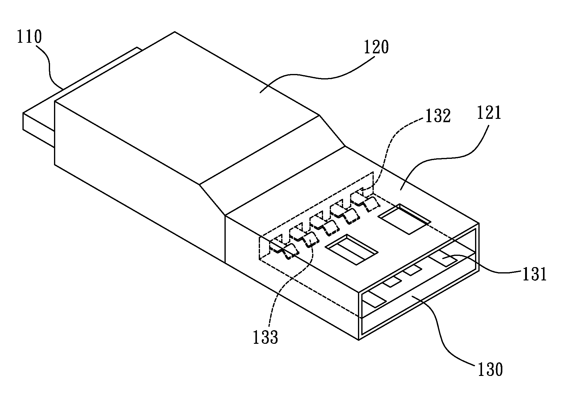
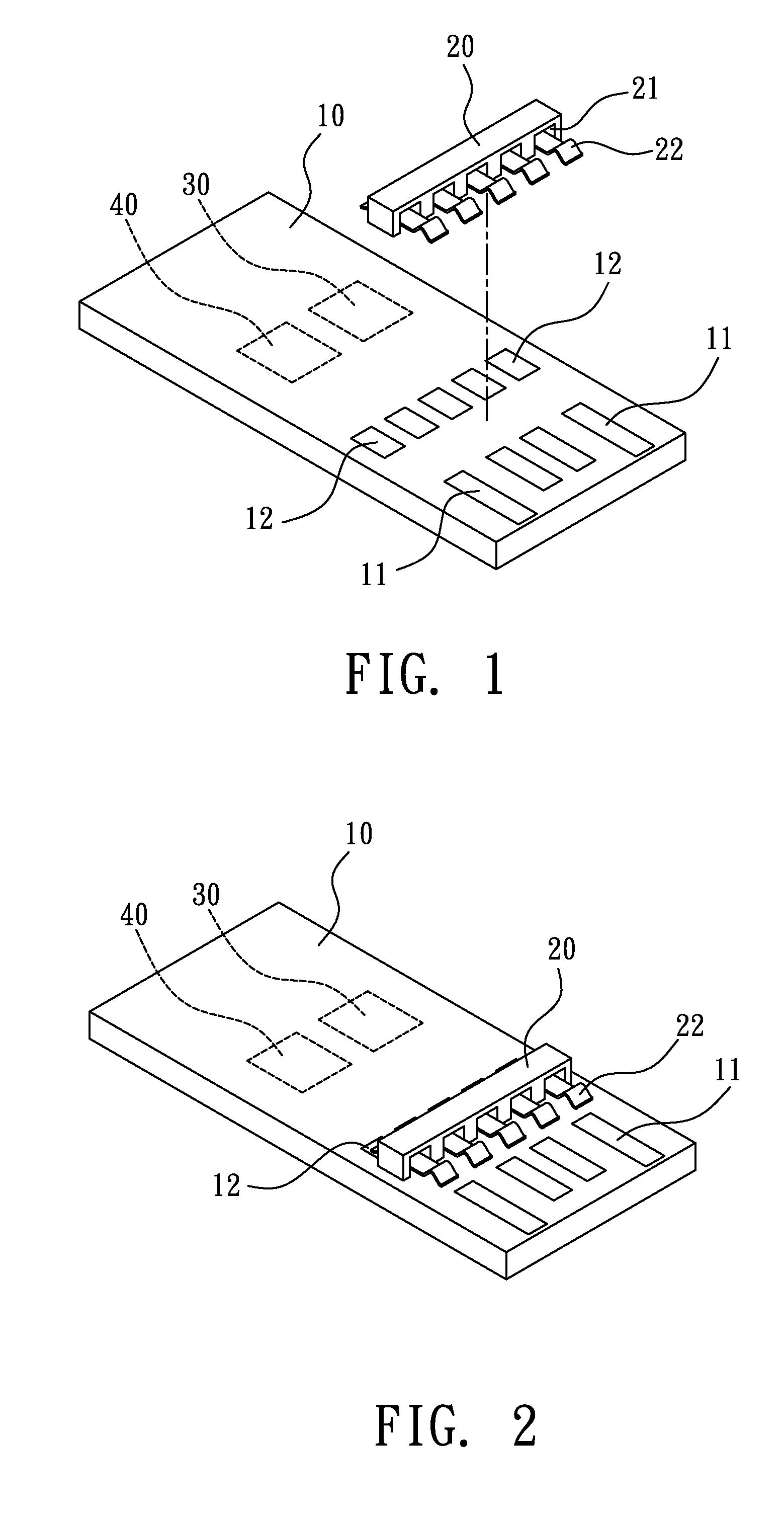
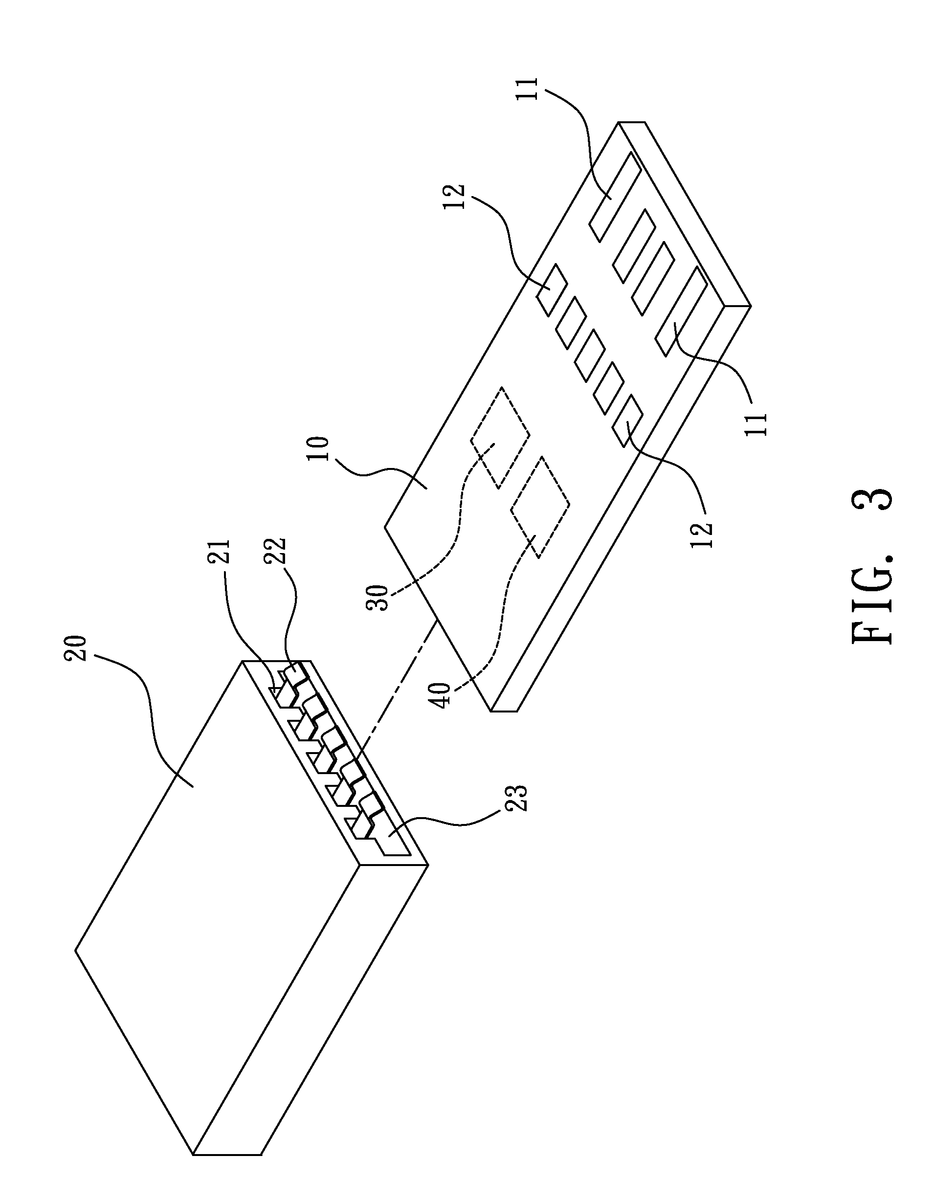
[0026]Referring to FIG. 1 and FIG. 2, wherein FIG. 1 is a schematic exploded view of the USB connector of one preferred embodiment of the present invention; and FIG. 2 is a schematic assembled view of the USB connector of one preferred embodiment of the present invention.
[0027]As shown in figures, the USB connector provided by the present invention comprises: a substrate 10, and a connector main body 20.
[0028]The substrate 10 is installed with a plurality of first contact pads 11 and a plurality of second contact pads 12 exposed outside the substrate 10, and the substrate 10 is a, e.g. but not limited to, Chip-On-Board (COB) substrate or printed circuit board substrate; in this embodiment of the present invention, the COB substrate is adopted for illustration and not served as a limitation. The COB technology has properties of thin thickness, compact wiring and small area, so it is widely used in the package of LCD driving chips or NAND flash memories.
[0029]The quantity of the plura...
PUM
 Abstract
Description
Claims
Application Information
 - Generate Ideas
- Intellectual Property
- Life Sciences
- Materials
- Tech Scout
- Unparalleled Data Quality
- Higher Quality Content
- 60% Fewer Hallucinations
Browse by: Latest US Patents, China's latest patents, Technical Efficacy Thesaurus, Application Domain, Technology Topic, Popular Technical Reports.
© 2025 PatSnap. All rights reserved.Legal|Privacy policy|Modern Slavery Act Transparency Statement|Sitemap|About US| Contact US: help@patsnap.com