

Layered inorganic nanocrystal photovoltaic devices
a nanocrystal and photovoltaic technology, applied in the field of solar cell devices, can solve the problems of high energy consumption, large amount of energy required, and large amount of incident solar energy spectrum
- Summary
- Abstract
- Description
- Claims
- Application Information
AI Technical Summary
Benefits of technology
Problems solved by technology
Method used
Image

Examples
Embodiment Construction
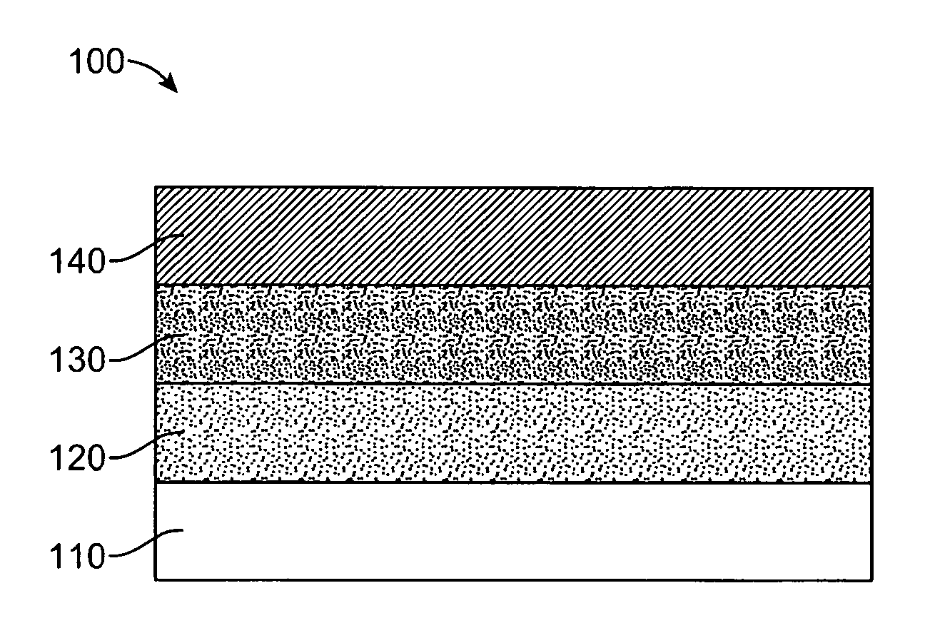
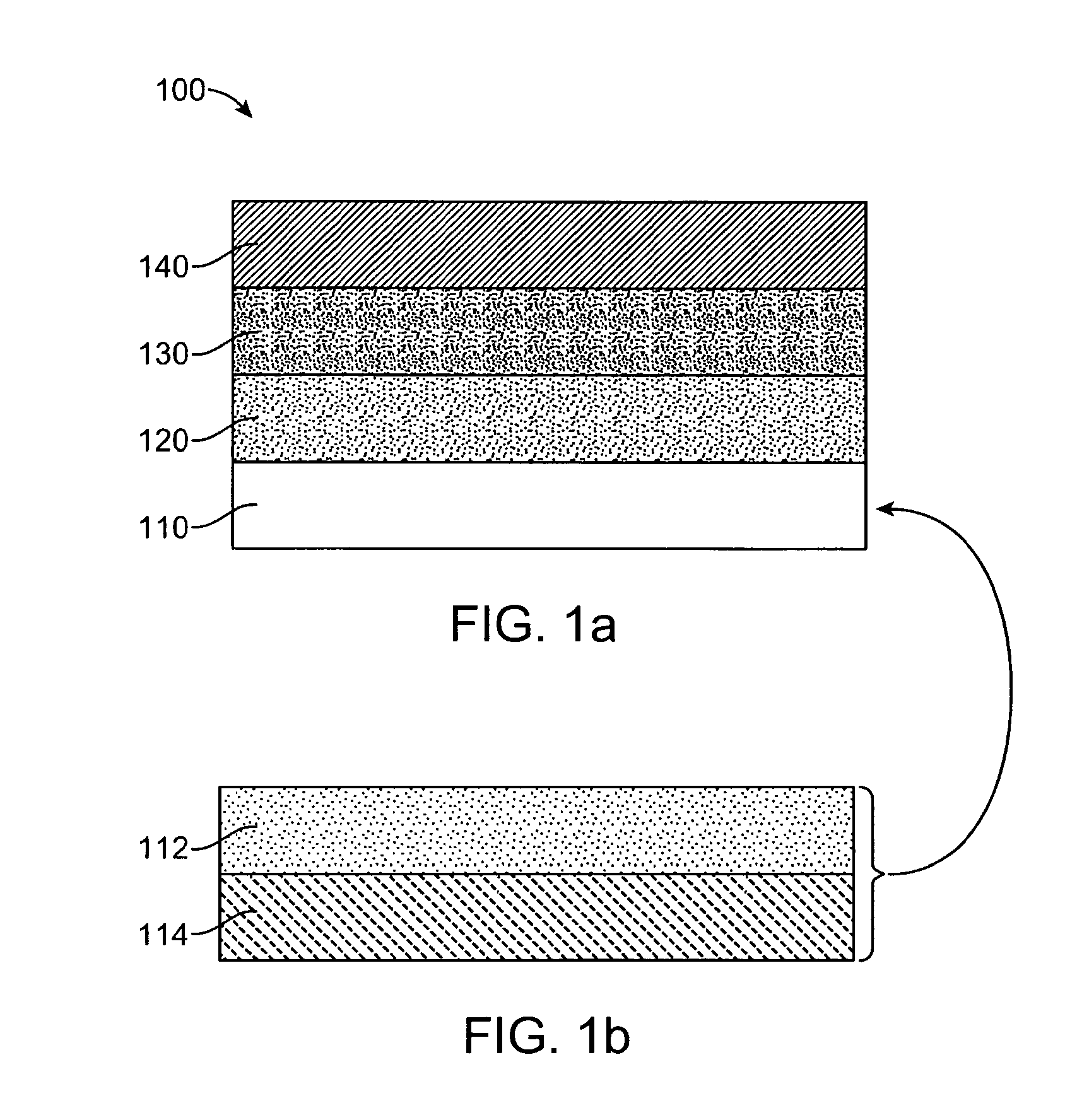
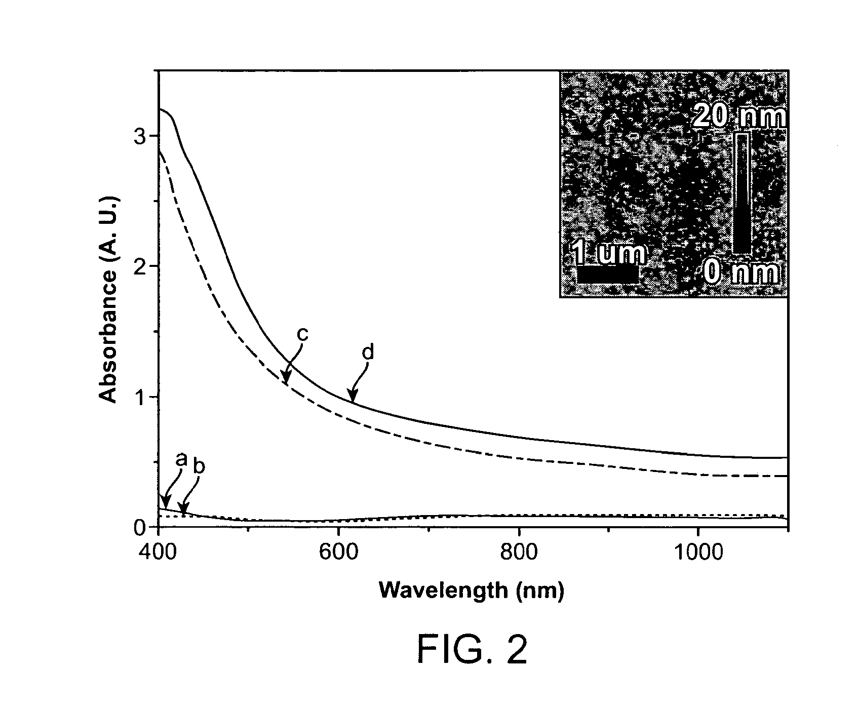
[0022]The aforementioned needs are satisfied by the embodiments of the present invention wherein a new approach to the colloidal synthesis of nanocrystals such as chalcocite (Cu2S) has been discovered, and this material has been successfully deployed in a working photovoltaic device.
[0023]Reference will now be made in detail to specific embodiments of the invention. Examples of the specific embodiments are illustrated in the accompanying drawings. While the invention will be described in conjunction with these specific embodiments, it will be understood that it is not intended to limit the invention to such specific embodiments. To the contrary, it is intended to cover alternatives, modifications, and equivalents as may be included within the scope of the appended claims. In the following description, numerous specific details are set forth in order to provide a thorough understanding embodiments of the present invention. Embodiments of the present invention may be practiced without...
PUM
| Property | Measurement | Unit |
|---|---|---|
| temperature | aaaaa | aaaaa |
| temperature | aaaaa | aaaaa |
| diameter | aaaaa | aaaaa |
Abstract
Description
Claims
Application Information