Functionalized nanoparticles and method

a nanoparticle and functional technology, applied in the field of nanoparticles, can solve the problems of limiting the technique to biological tagging and imaging, reducing the emission efficiency and stability, and limiting the technique to aqueous based applications

Active Publication Date: 2010-11-11
SAMSUNG ELECTRONICS CO LTD
View PDF99 Cites 89 Cited by
  • Summary
  • Abstract
  • Description
  • Claims
  • Application Information

AI Technical Summary

Benefits of technology

[0007]The present invention relates to nanoparticles including one or more ligands attached to a surface of the nanop...

Problems solved by technology

These procedures can be detrimental to maintaining the optical properties of the quantum dots and often result in drastically reduced emission efficiencies and stability,
The drawback of these met...

Method used


Image

  • Functionalized nanoparticles and method
  • Functionalized nanoparticles and method
  • Functionalized nanoparticles and method

Examples


example 1a

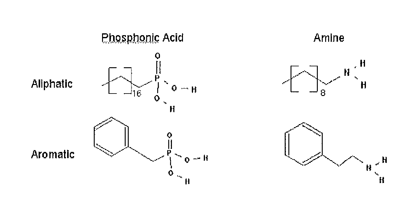
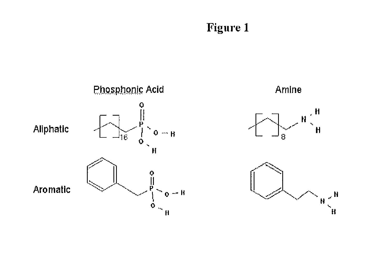
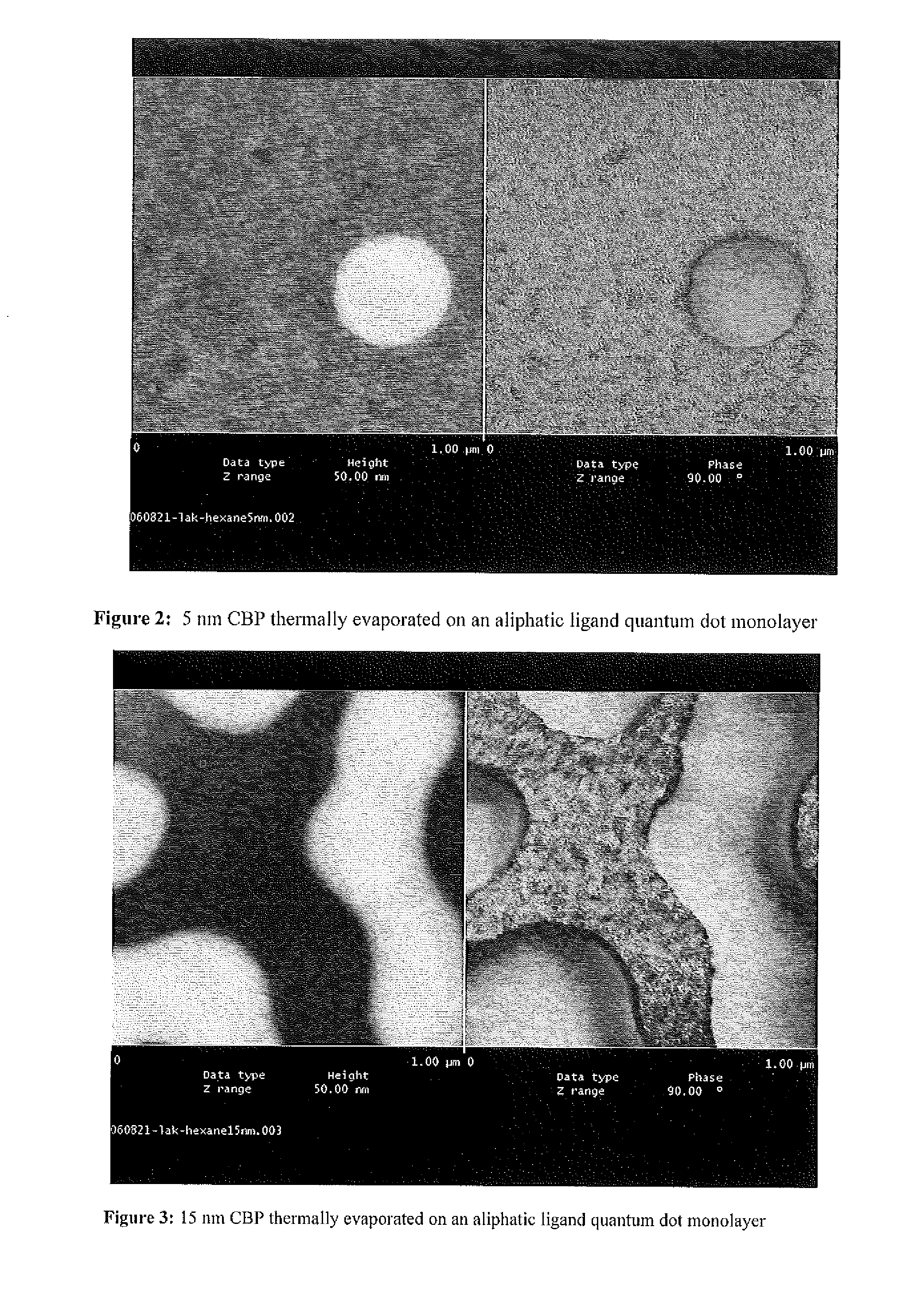
[0182]Performing the overcoating procedure with TOPO as the solvent, replacing the existing aliphatic phosphonic acid and amine species with aromatic derivatives (see FIG. 1) results in semiconductor nanocrystals that have new surface chemistry while maintaining their optical properties. These semiconductor nanocrystals are no longer soluble in hexane, but are readily soluble in toluene and chloroform. In addition, thin films of organic molecules can be reliably deposited onto ordered films of these synthetically modified nanocrystals without the “puddling” associated with traditional aliphatic semiconductor nanocrystal surface chemistry (see FIGS. 2-5). It is believed that a phosphonic acid / amine salt is the predominant species on the surface of the semiconductor nanocrystal despite the fact that TOPO is in large excess during the reaction.

[0183]Preparation of Aromatic Semiconductor Nanocrystals Capable of Emitting Red Light

[0184]Synthesis of Cc / Se Cores: 1 mmol cadmium acetate was...

example 1-b

[0188]Preparation of Semiconductor Nanocrystals Capable of Emitting Green Light

[0189]Synthesis of ZnSe Cores: 0.69 mmol diethyl zinc was dissolved in 5 ml, of tri-n-octylphosphine and mixed with 1 mL of 1 M TBP-Se, 28.9 mmol of Oleylamine was loaded into a 3-neck flask, dried and degassed at 90° C. for one hour. After degassing, the flask was heated to 310° C. under nitrogen. Once the temperature reached 310° C., the Zn solution was injected and the reaction mixture was heated at 270° C. for 15-30 minutes while aliquots of the solution were removed periodically in order to monitor the growth of the nanocrystals. Once the first absorption peak of the nanocrystals reached 350 nm, the reaction was stopped by dropping the flask temperature to 160° C. and used without further purification for preparation of CdZnSe cores.

[0190]Synthesis of CdZnSe Cores: 1.12 mmol dimethylcadmium was dissolved in 5 mL of tri-n-octylphosphine and mixed with 1 mL of 1 M TBP-Se. In a 4-neck flask, 41.38 mmol ...

example 1-c

[0192]Preparation of Semiconductor Nanocrystals Capable of Emitting Red Light

[0193]Synthesis of CdSe Cores: 1 mmol cadmium acetate was dissolved in 8.96 mmol of tri-n-octylphosphine at 100° C. in a 20 mL vial and then dried and degassed for one hour. 15.5 mmol of trioctylphosphine oxide and 2 mmol of octadecylphosphonic acid were added to a 3-neck flask and dried and degassed at 140° C. for one hour. After degassing, the Cd solution was added to the oxide / acid flask and the mixture was heated to 270° C. under nitrogen. Once the temperature reached 270° C., 8 mmol of tri-n-butylphosphine was injected into the flask. The temperature was brought back to 270° C. where 1.1 mL of 1.5 M TBP-Se was then rapidly injected. The reaction mixture was heated at 270° C. for 15-30 minutes while aliquots of the solution were removed periodically in order to monitor the growth of the nanocrystals. Once the first absorption peak of the nanocrystals reached 565-575 nm, the reaction was stopped by cooli...


PUM


Abstract

A nanoparticle including an inorganic core comprising at least one metal and/or at least one semi-conductor compound comprising at least one metal includes a coating or shell disposed over at least a portion of a surface of the core. The coating can include one or more layers. Each layer of the coating can comprise a metal and/or at least one semiconductor compound. The nanoparticle further includes a ligand attached to a surface of the coating. The ligand is represented by the formula: X-Sp-Z, wherein X represents, e.g., a primary amine group, a secondary amine group, a urea, a thiourea, an imidizole group, an amide group, a phosphonic or arsonic acid group, a phosphinic or arsinic acid group, a phosphate or arsenate group, a phosphine or arsine oxide group; Sp represents a spacer group, such as a group capable of allowing a transfer of charge or an insulating group; and Z represents: (i) reactive group capable of communicating specific chemical properties to the nanocrystal as well as provide specific chemical reactivity to the surface of the nanocrystal, and/or (ii) a group that is cyclic, halogenated, or polar a-protic. In certain embodiments, at least two chemically distinct ligands are attached to an surface of the coating, wherein the at least two ligands (I and II) are represented by the formula: X-Sp-Z. In ligand (I) X represents a phosphonic, phosphinic, or phosphategroup and in ligand (II) X represents a primary or secondary amine, or an imidizole, or an amide; In both ligands (I) and (II) Sp, which can be the same or different in the two compounds, represents a spacer group, such as a group capable of allowing a transfer of charge or an insulating group; Z, which can be the same or different in the two compounds, is a group chosen from among groups capable of communicating specific chemical properties to the nanoparticle as well as provide specific chemical reactivity to the surface of the nanoparticle. In preferred embodiments, the nanoparticle includes a core comprising a semiconductor material.

Description

[0001]This application is a continuation of commonly owned International Application No. PCT / US2008 / 010651 filed 12 Sep. 2008, which was published in the English language as PCT Publication No. WO 2009 / 035657 on 19 Mar. 2009, which International Application claims priority to U.S. Application No. 60 / 971,887, filed 12 Sep. 2007; 60 / 992,598, filed 5 Dec. 2007; and 61 / 083,998, filed 28 Jul. 2008; each of the foregoing hereby being incorporated herein by reference in its entirety.[0002]International Application No, PCT / US2008 / 010651 further claims priority to U.S. Application No. 60 / 971,885, filed 12 Sep. 2007; 60 / 973,644, filed 19 Sep. 2007; and 61 / 016,227, filed 21 Dec. 2007. International Application No. PCT / US2008 / 010651 is also a continuation-in-part application of commonly owned International Application No. PCT / US2007 / 024750, filed 3 Dec. 2007. International Application No. PCT / US2008 / 010651 is also a continuation-in-part application of commonly owned International Application No...

Claims


Application Information

Patent Timeline
IPC IPC(8): H01B1/02
CPCB82Y30/00C09K11/565C09K11/881G01N33/587C30B29/605C30B33/00G01N33/54346C09K11/883C09K11/025B82Y20/00Y10S977/774Y10S977/95
Inventor BREEN, CRAIGCOX, MARSHALLSTECKEL, JONATHAN S.
Owner SAMSUNG ELECTRONICS CO LTD
Why Eureka
Try Eureka