Method for preparing multilayer of nanocrystals, and organic-inorganic hybrid electroluminescence device comprising multilayer of nanocrystals prepared by the method

a nanocrystal and hybrid technology, applied in the direction of discharge tube/lamp details, crystal growth process, natural mineral layered products, etc., can solve the problems of not specifically describing the process of forming a monolayer of nanocrystals or preparing a multilayer of nanocrystals using the monolayer, and the overall procedure is rendered more complex. , to achieve the effect of simple manner

Active Publication Date: 2006-03-23
SAMSUNG ELECTRONICS CO LTD
View PDF12 Cites 91 Cited by
  • Summary
  • Abstract
  • Description
  • Claims
  • Application Information

AI Technical Summary

Benefits of technology

[0015] Thus, the present inventors have earnestly and intensively conducted research to solve the problems of conventional methods for preparing a multilayer of nanocrystals in terms of complicated procedures. As a result, the present inventors have found that when nanocrystals surface-coordinated by a photosensitive compound are coated on a substrate and exposed to UV light, a crosslinking reaction takes place between photosensitive functional groups of the photosensitive compound to form a network structure, resulting in the formation of a monolayer of nanocrystals insoluble in solvents, and further the preparation of a multilayer of nanocrystals in a relatively simple manner when compared to prior art methods. The present invention is based on this finding.

Problems solved by technology

However, these methods for forming a thin film of nanocrystals by self-assembly have a problem that they involve an additional step of treating the surface of nanocrystals and a substrate with a compound containing a specific functional group, rendering the overall procedure more complex.
However, the patent publication simply describes that the multilayer of nanocrystals can be prepared by the use of a self-assembly process mentioned in U.S. Pat. No. 5,751,018, but fails to specifically describe a process for forming a monolayer of nanocrystals or preparing a multilayer of nanocrystals using the monolayer.
However, the luminescence device is not driven by electroluminescence.

Method used


Image

  • Method for preparing multilayer of nanocrystals, and organic-inorganic hybrid electroluminescence device comprising multilayer of nanocrystals prepared by the method
  • Method for preparing multilayer of nanocrystals, and organic-inorganic hybrid electroluminescence device comprising multilayer of nanocrystals prepared by the method
  • Method for preparing multilayer of nanocrystals, and organic-inorganic hybrid electroluminescence device comprising multilayer of nanocrystals prepared by the method

Examples


example 1

Preparation of Multilayer of CdSeS Nanocrystals Surface-Coordinated by Photosensitive Compound

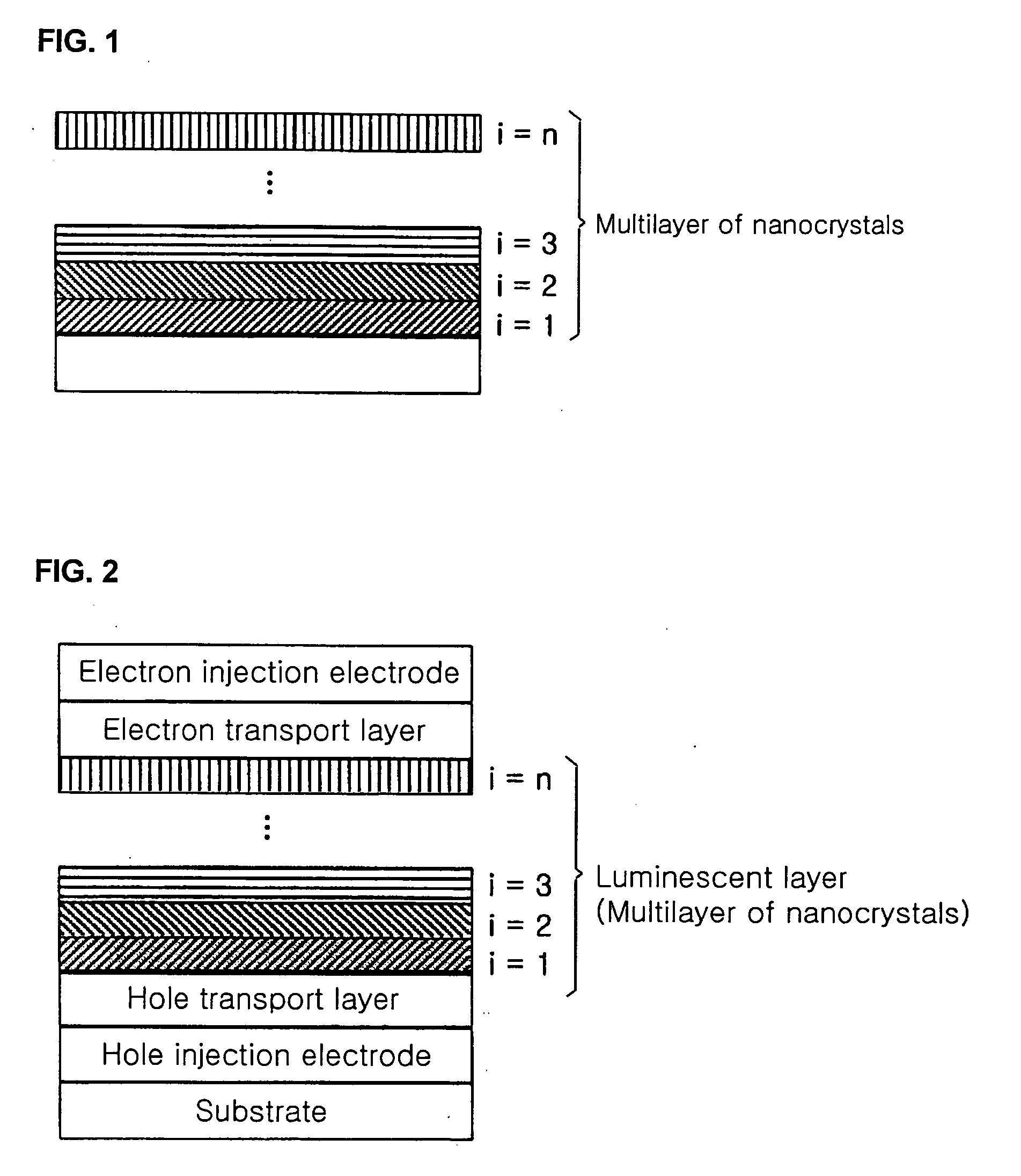
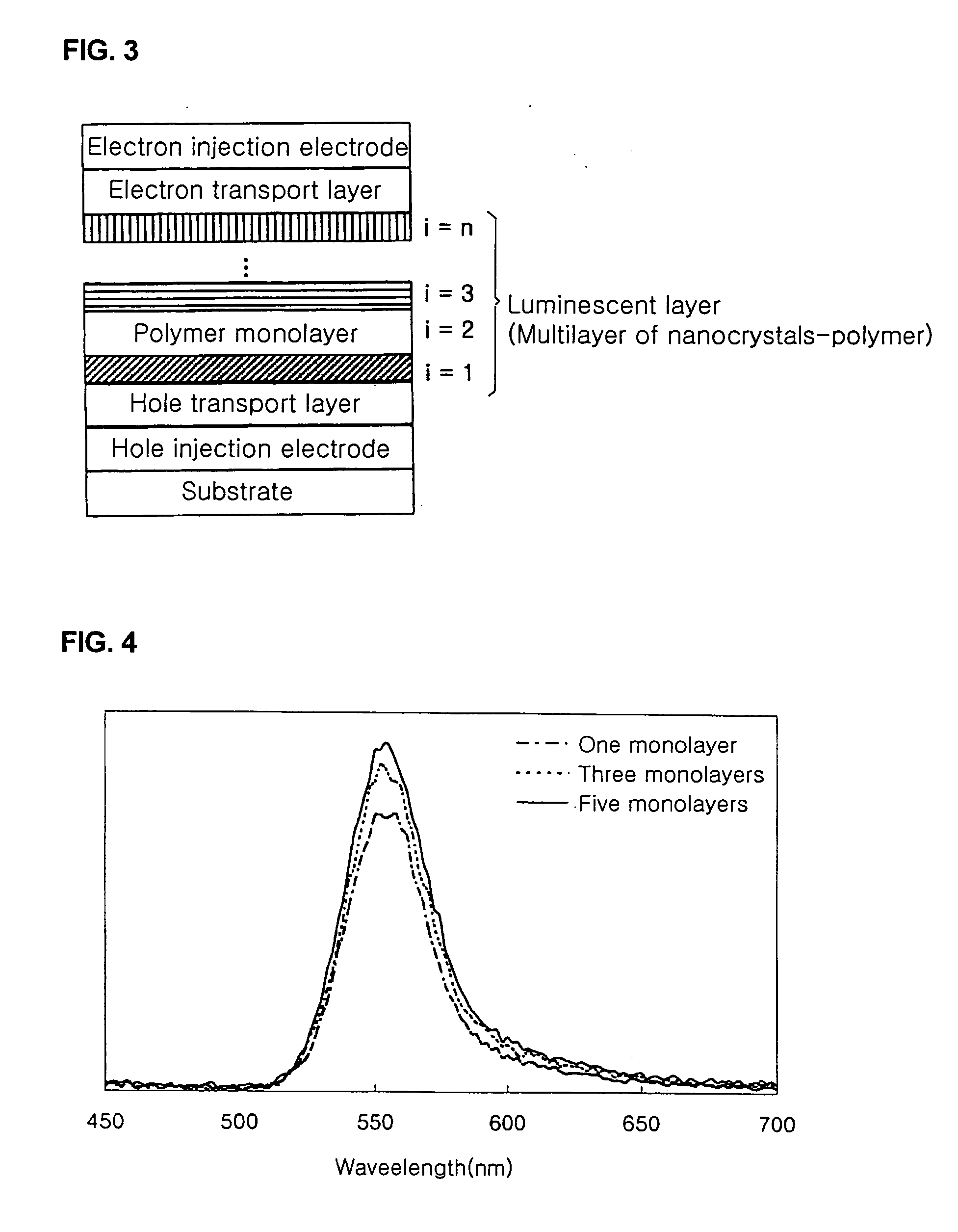
[0065] After the toluene dispersion of CdSeS nanocrystals (1 wt %) prepared in Preparative Example 1 was dropped onto a glass substrate cleaned with isopropyl alcohol (IPA), spin coating was performed at 2,000 rpm for 30 seconds. The coated glass substrate was heated on a heating plate at 50° C. to form a monolayer of the nanocrystals. The monolayer was placed in a UV exposure system at an effective wavelength of 200˜300 nm, and then UV light (800 W) was irradiated to the monolayer for about 300 seconds. The toluene dispersion of nanocrystals was dropped onto the UV-exposed monolayer, which was then spin-coated, dried and exposed to UV light under the same conditions as the previous formation procedure of the monolayer of nanocrystals. Thereafter, this procedure was repeated four times to prepare a multilayer (5-layer) of nanocrystals. FIG. 4 shows photoluminescence spectra of the multilay...

example 2

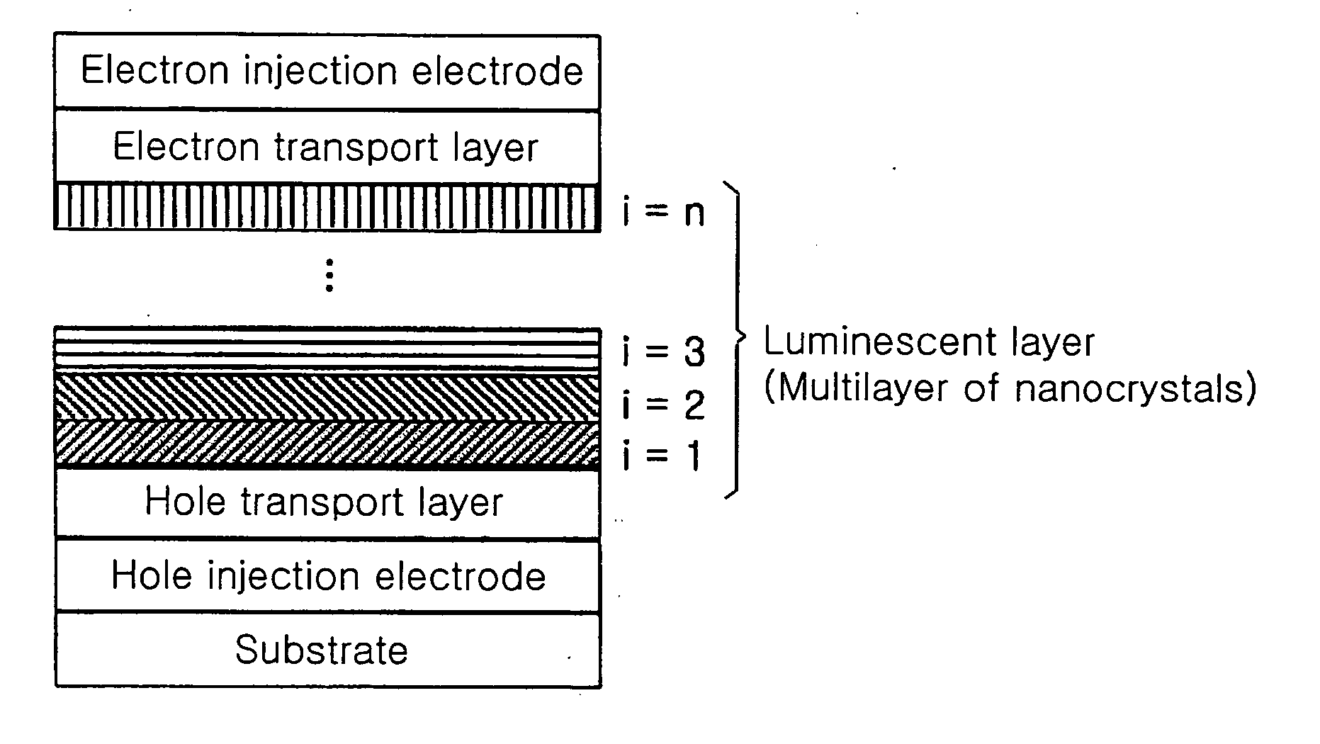
Fabrication of Electroluminescence Device Comprising Multilayer of Nanocrystals-Polymer as Luminescent Layer

[0066] An ITO-patterned glass substrate was sequentially washed with a neutral detergent, deionized water, acetone and isopropyl alcohol, and was then subjected to UV-ozone treatment. Poly(9,9′-dioctylfluorene-co-N-(4-butylphenyl)diphenylamine (TFB) was spin-coated on the substrate to form a hole transport layer having a thickness of 50 nm, and then baked. The toluene solution of CdSeS nanocrystals (1 wt %) prepared in Preparative Example 1 was spin-coated on the hole transport layer and dried to form a monolayer having a thickness of about 5 nm. After the monolayer was placed in a UV exposure system at an effective wavelength of 200˜300 nm, UV (800 W) light was irradiated thereto for about 200 seconds. A solution of TFB was spin-coated on the exposed monolayer, and baked to obtain a polymer monolayer. The CdSeS nanocrystals were spin-coated on the polymer monolayer to prepar...


PUM

PropertyMeasurementUnit
wavelengthaaaaaaaaaa
melting pointaaaaaaaaaa

Abstract

A method for preparing a multilayer of nanocrystals. The method includes the steps of (i) coating nanocrystals surface-coordinated by a photosensitive compound, or a mixed solution of a photosensitive compound and nanocrystals surface-coordinated by a material miscible with the photosensitive compound, on a substrate, drying the coated substrate, and exposing the dried substrate to UV light to form a first monolayer of nanocrystals, and (ii) repeating the procedure of step (i) to form one or more monolayers of nanocrystals on the first monolayer of nanocrystals. Further, an organic-inorganic hybrid electroluminescence device using a multilayer of nanocrystals prepared by the method as a luminescent layer. The luminescent efficiency and luminescence intensity of the electroluminescence device can be enhanced, and the electrical properties of the electroluminescence device can be controlled by the use of the multilayer of nanocrystals as a luminescent layer.

Description

[0001] This non-provisional application claims priority under 35 U.S.C. 119(a) on Korean Patent Application No. 2004-38391 filed on May 28, 2004, which is herein expressly incorporated by reference. BACKGROUND OF THE INVENTION [0002] 1. Field of the Invention [0003] The present invention relates to a method for preparing a multilayer of nanocrystals, and an organic-inorganic hybrid electroluminescence device comprising a multilayer of nanocrystals prepared by the method. More particularly, the present invention relates to a method for preparing a multilayer of nanocrystals by (i) coating nanocrystals surface-coordinated by a photosensitive compound, or a mixed solution of a photosensitive compound and nanocrystals surface-coordinated by a material miscible with the photosensitive compound, on a substrate, drying the coated substrate, and exposing the dried substrate to UV light to form a first monolayer of nanocrystals, and (ii) repeating the procedure of (i) to form one or more mon...

Claims


Application Information

Patent Timeline
Patent Type & Authority Applications(United States)
IPC IPC(8): H01L51/54H05B33/14C09K11/00B05D3/00H05B33/10C09K11/06C09K11/54C09K11/56C09K11/60C09K11/62C09K11/64C09K11/66C09K11/68C09K11/70C09K11/74C09K11/87C09K11/88C09K11/89H01L33/08
CPCB82Y20/00Y10T428/256C09K11/025C09K11/565C09K11/62C09K11/621C09K11/64C09K11/661C09K11/70C09K11/7492C09K11/88C09K11/883C09K11/892H01L51/5012H05B33/14B82Y30/00H10K50/13H10K50/115H10K50/11B82Y40/00G02F1/133614C30B7/14C30B29/48G02B6/005
Inventor JANG, EUN JOOJUN, SHIN AELEE, SUNG HUNPARK, JONG JINCHOI, SEONG JAEAHN, TAE KYUNG
Owner SAMSUNG ELECTRONICS CO LTD
Why Eureka
Try Eureka