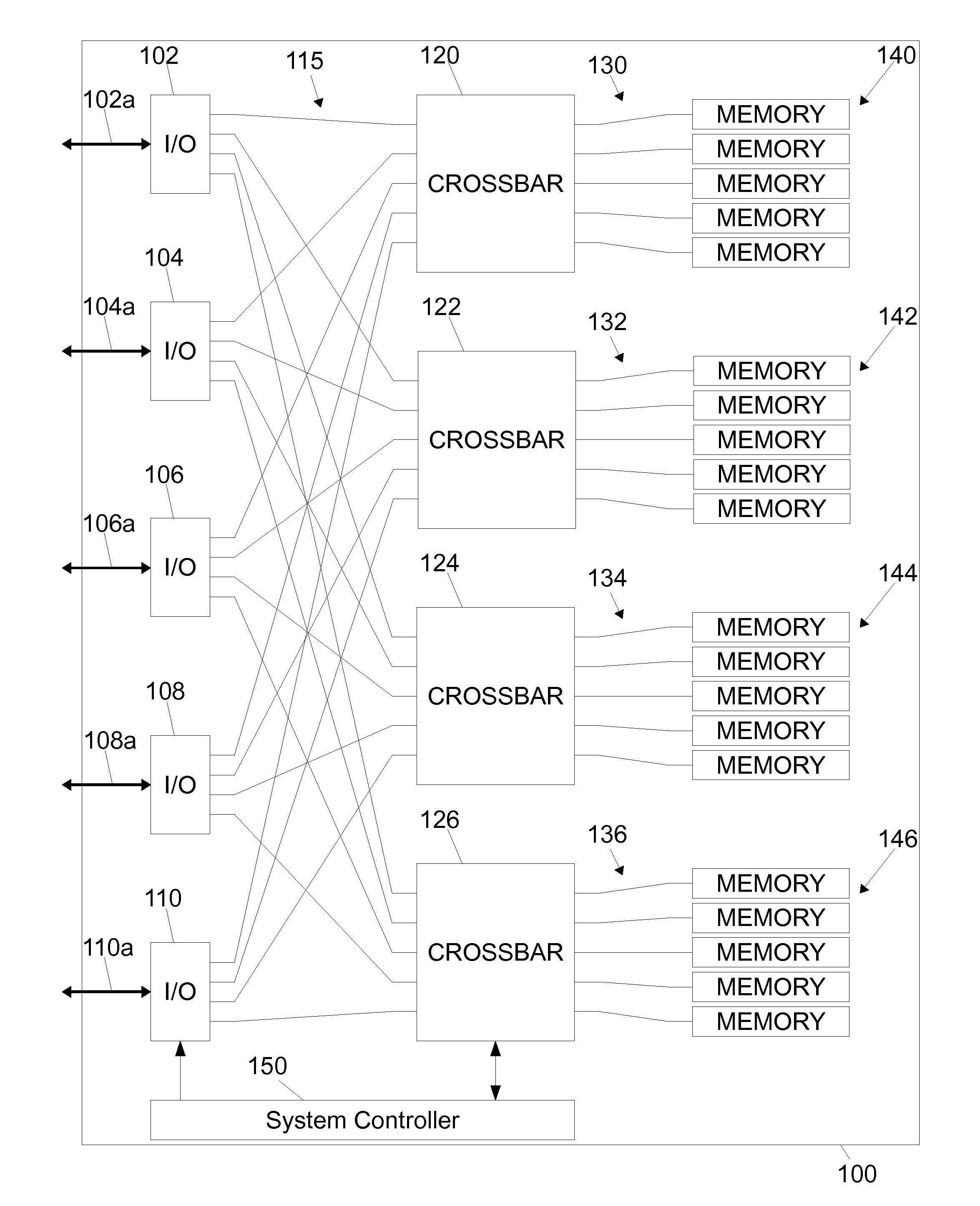
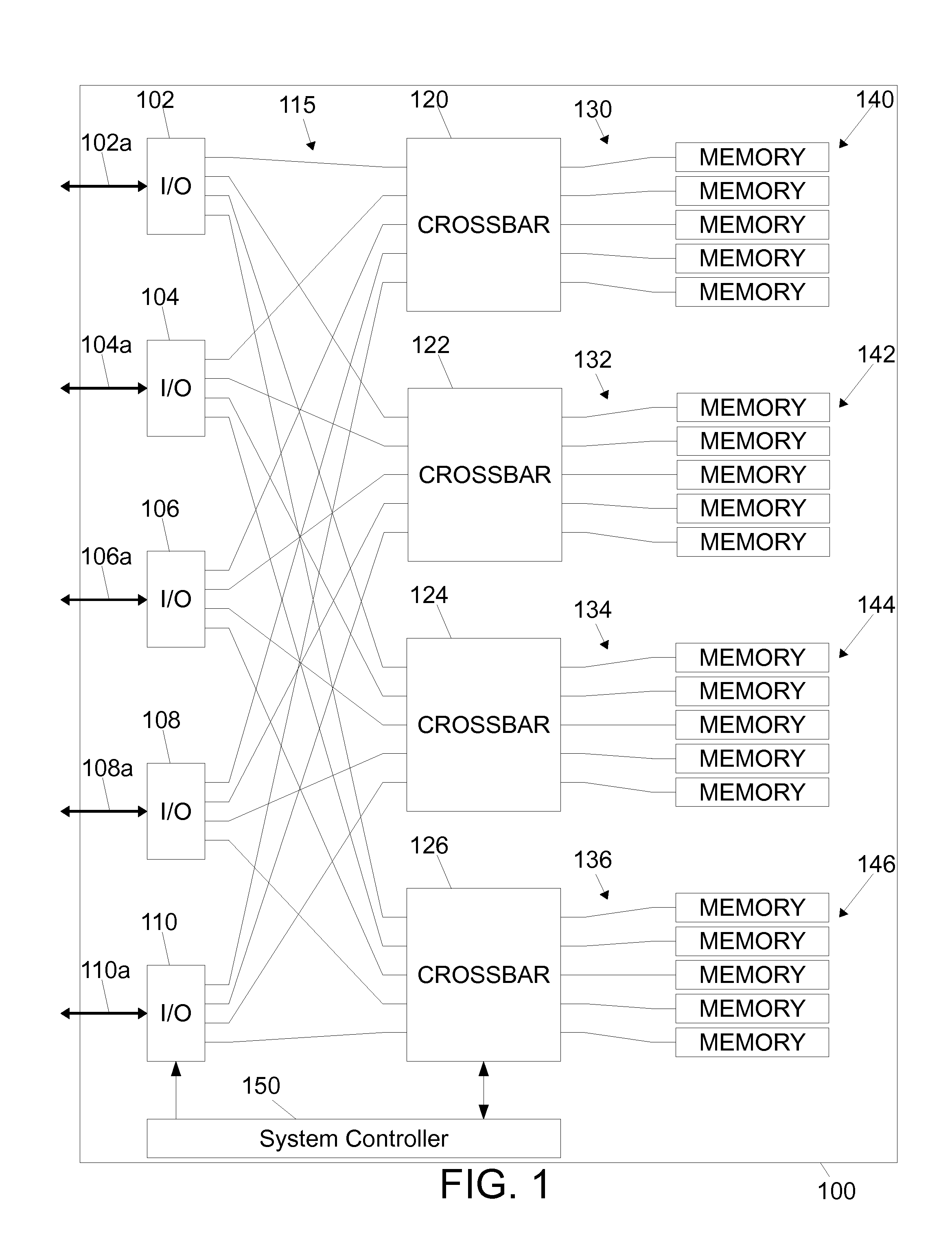
[0009]The disclosed embodiments relate to methods and apparatuses for providing a more effective, efficient, and optimal high-speed memory system. In general, in one aspect, the disclosed embodiments relate to a Flash-based memory module having high-speed serial communication. The Flash-based memory module comprises, among other things, a plurality of input / output (I / O) modules, each I / O module configured to communicate with an external device over one or more external communication links, a plurality of Flash-based memory cards, each Flash-based memory card comprising a plurality of Flash memory devices, each Flash memory device having a physical memory space that is divided into blocks, each block being further divided into pages, each page representing an individually addressable memory location on which memory operations are performed, multiple such memory locations being erasable at the same time in one-block groupings, and a plurality of crossbar switching elements, each crossbar switching element being connected to a respective one of the Flash-based memory cards and configured to allow each one of the I / O modules to communicate with the respective one of the Flash-based memory cards. Each I / O module is connected to each crossbar switching element by a high-speed serial communication link, each high-speed serial communication link allowing each I / O module to transmit and receive bits representing commands, instructions and / or data to and from each crossbar switching element, and each crossbar switching element is connected to the respective one of the Flash-based memory cards by a plurality of parallel communication links, each parallel communication link connecting one crossbar switching element to one of the Flash memory devices of the respective one of the Flash-based memory cards.
[0010]In general, in another aspect, the disclosed embodiments relate to an expandable high-speed memory. The expandable high-speed memory comprises, among other things, a printed circuit board (PCB), interface circuitry mounted on the PCB and configured to allow the high-speed memory card to receive bits representing instructions, commands, and / or data from one or more external devices over one or more high-speed serial communication links, a plurality of memory devices mounted to the PCB, each memory device having a physical memory space on which memory operations are performed, and a controller mounted to the PCB and connected to the interface circuitry and the plurality of memory devices, the controller configured to control communication between the interface circuitry and each memory device to perform the memory operations. The interface circuitry is connected to the controller by a plurality of high-speed serial communication lines, each high-speed serial communication line corresponding to one of the high-speed serial communication links, and the controller is connected to the plurality of memory devices by a predefined number of parallel communication lines, the controller configured to convert the bits representing commands, instructions and / or data from the high-speed serial communication links from a serial format to a parallel format.
[0011]In general, in yet another aspect, the disclosed embodiments relate a memory module having high-speed serial communication. The memory module comprises, among other things, a first plurality of input processing blocks and a second plurality of input processing blocks, each input processing blocks configured to receive bits representing commands, instructions and / or data according to a serial format and rearrange the bits representing commands, instructions and / or data according to a parallel format, a plurality of memory devices, each memory device having a physical memory space on which memory operations are performed, and a controller connected to the first and second plurality of input processing blocks and the memory devices, the controller configured to control communication between the first and second plurality of input processing blocks and each memory device to perform the memory operations. The controller comprises, among other things: (a) a first multi-channel buffer and a second multi-channel buffer connected to the first and second plurality of input processing blocks, respectively, each multi-channel buffer configured to receive the bits representing commands, instructions and / or data in parallel format from the first and second plurality of input processing blocks, respectively, and construct a predefined number of words from the bits representing commands, instructions and / or data, each word being composed of a predefined number of bits; (b) a first error correction and data protection circuit and a second error correction and data protection circuit connected to the first and second multi-channel buffers, respectively, the first and second error correction and data protection circuits configured receive the words from the first and second multi-channel buffer, respectively, generate one or more error correction code bits using the words, add the error correction code bits for each word to the word, and output each word with the error correction code bits added thereto; (c) a first output buffer and a second output buffer connected to the first and second correction and data protection circuits, respectively, the first and second output buffers configured to receive in turn the words with the error correction code bits added thereto from the first and second error correction and data protection circuits such that a first word from one of the first and second error correction and data protection circuits is provided to one of the first and second output buffers and a next word from another one of the first and second error correction and data protection circuits is provided to another one of the first and second output buffers; and (d) a memory buffer configured to received the words with the error correction code bits added thereto from the first and second output buffers and to combine a predefined number of the words in a predefined manner to form a super-word.

