Systems and methods for manufacturing passive waveguide components

a technology of passive waveguide components and manufacturing methods, applied in waveguide type devices, instruments, optical elements, etc., can solve the problems of high cost, large market price fluctuations, and high cost of cnc machine and die-cast processing, and achieve the effect of manufacturing, and reducing the cost of machining

Active Publication Date: 2012-04-12
AVIAT U S
View PDF3 Cites 45 Cited by
  • Summary
  • Abstract
  • Description
  • Claims
  • Application Information

AI Technical Summary

Benefits of technology

[0009]In some embodiments, the method may further comprise trimming or polishing the non-conductive structure or the conductive layer. For some embodiments, the conductive layer may have a thickness that enables or creates the electrical feature of the passive waveguide component to function within an accepted parameter. For example, the conductive layer may have a thickness that enables the conductive layer to benefit from skin effect and permit the bulk of a current operating at radio or microwave frequencies ...

Problems solved by technology

Unfortunately, traditional manufacturing processes for waveguide components suffer from several drawbacks.
One such drawback is that CNC machine and die-cast processing tend to be expensive and require an operator with considerable skill (e.g., a trained machinist).
Another drawback is that the metals typically used in traditional waveguide components are susceptible to large market price fluctuations due to global supply and demand.
Another drawback is that with conventional waveguide manufacturing, waveguide components are unable to be produced on an “on-deman...

Method used


Image

  • Systems and methods for manufacturing passive waveguide components
  • Systems and methods for manufacturing passive waveguide components
  • Systems and methods for manufacturing passive waveguide components

Examples


Embodiment Construction

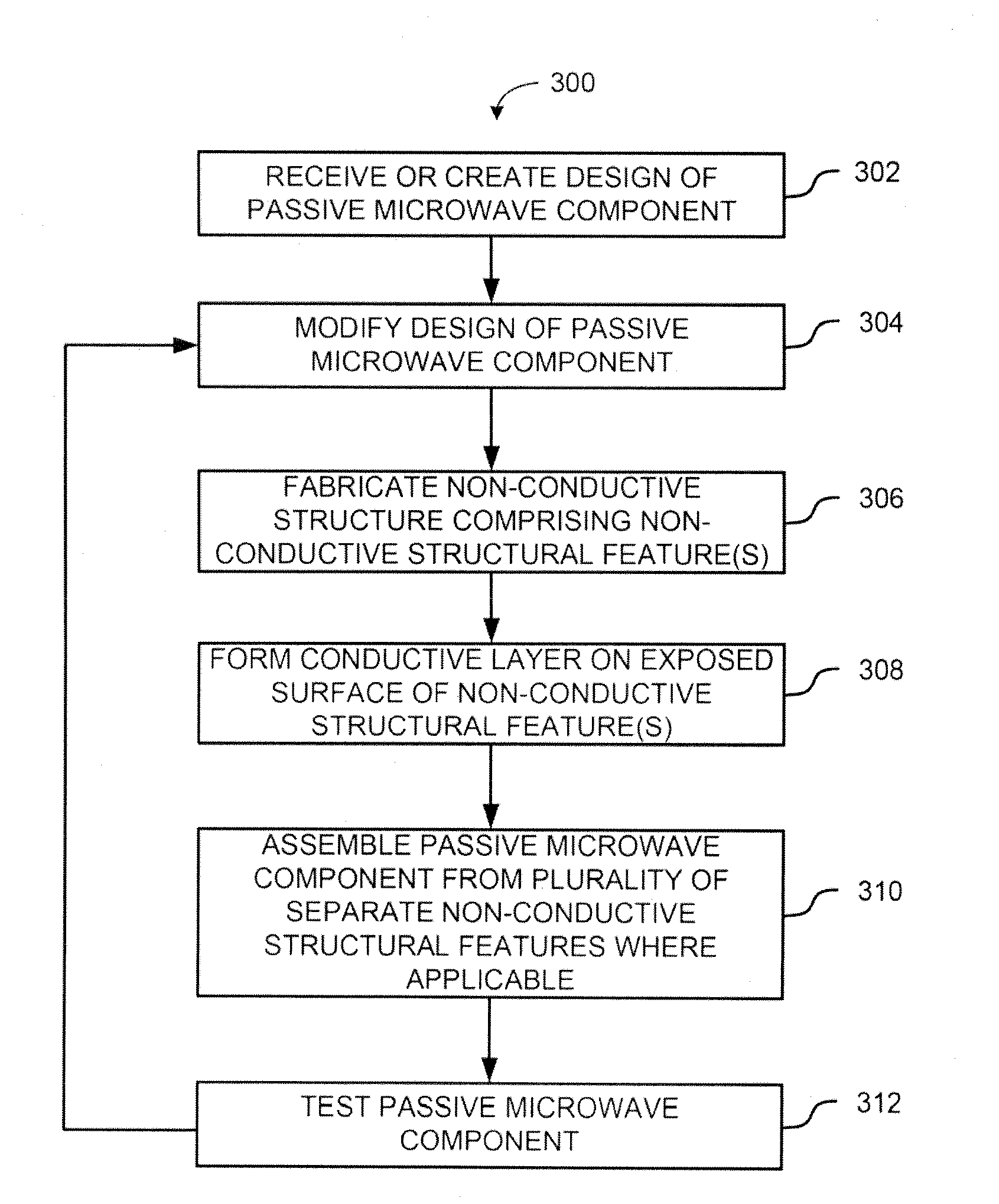
[0006]Various embodiments provide for systems and method for manufacturing low cost passive waveguide components, such as passive waveguide components.

[0007]According to some embodiments, a method for manufacturing a passive waveguide component is provided. The method may comprise receiving a design for the passive waveguide component, receiving a non-conductive material, fabricating a non-conductive structure of the passive waveguide component based on the design, wherein the non-conductive structure comprises the non-conductive material, and forming a conductive layer on an exposed surface of at least one non-conductive structural feature of the non-conductive structure to create an electrical feature of the passive waveguide components.

[0008]Depending on the embodiment, fabricating the non-conductive structure based on the design may comprise fabricating the non-conductive structure using three-dimensional (3D) printing or plastic injection molding, and the non-conductive materia...


PUM

PropertyMeasurementUnit
Thicknessaaaaaaaaaa
Electrical conductoraaaaaaaaaa

Abstract

Various embodiments are directed toward systems and method for manufacturing low cost passive waveguide components. For example, various embodiments relate to low cost manufacturing of passive waveguide components, including without limitation, waveguide filters, waveguide diplexers, waveguide multiplexers, waveguide bends, waveguide transitions, waveguide spacers, and an antenna adapter. Some embodiments comprise manufacturing a passive waveguide component by creating a non-conductive structure using a low cost fabrication technology, such as injection molding or three-dimensional (3D) printing, and then forming a conductive layer over the non-conductive structure such that the conductive layer creates an electrical feature of the passive waveguide component.

Description

CROSS-REFERENCE TO RELATED APPLICATIONS[0001]This application claims priority from U.S. Provisional Application Ser. No. 61 / 387,951 filed Sep. 29, 2010, entitled “Methods and Apparatus for Fabrication of Low Cost Passive Microwave Components,” which is hereby incorporated by reference.FIELD OF THE INVENTION(S)[0002]The present invention(s) relate to waveguide components, and more particularly, some embodiments relate to manufacturing passive waveguide components at reduced cost.DESCRIPTION OF THE RELATED ART[0003]Waveguide components are an integral component in many microwave communication systems. Generally, waveguide components consist of hollow metal pipes that are purposefully shaped and specifically dimensioned to guide and / or propagate an electromagnetic wave of a particular frequency from one end of the waveguide component to other. Traditionally, these waveguides components are manufactured using a Computer Numerically Controlled (CNC) machine process or a die-cast process,...

Claims


Application Information

Patent Timeline
IPC IPC(8): H05K13/00
CPCG02B6/125G02B6/138H01P11/001Y10T29/49002H03H7/468Y10T29/49117H03H3/00H01P11/003H01P11/002Y10T29/49016H03H3/007H01P1/207B33Y80/00B33Y70/00
Inventor NATH, JAYESHSHEN, YINGNEALIS, EDWIN
Owner AVIAT U S
Why Eureka
Try Eureka