Check patentability & draft patents in minutes with Patsnap Eureka AI!

Layered chip package and method of manufacturing same

Inactive Publication Date: 2012-04-12
HEADWAY TECH INC +1
View PDF4 Cites 70 Cited by
  • Summary
  • Abstract
  • Description
  • Claims
  • Application Information

AI Technical Summary

Benefits of technology

[0013]It is an object of the present invention to provide a layered chip package, a composite layered chip package, and methods of manufacturing the same that make it possible to stack a plurality of layered chip packages and electrically connect them to each other in a simple configuration, whereby a package including a desired number of semiconductor chips can be provided at low cost.
[0030]According to the layered chip package, the composite layered chip package, and the methods of manufacturing the same of the present invention, the plurality of first terminals and the plurality of second terminals can be used to stack and electrically connect a plurality of layered chip packages (subpackages). In the present invention, the first layer portion and the second layer portion are bonded to each other such that the respective second surfaces face each other. The plurality of first terminals are formed by using the plurality of surface electrodes of the first layer portion. The plurality of second terminals are formed by using the plurality of surface electrodes of the second layer portion. The present invention thus allows a plurality of layered chip packages (subpackages) to be electrically connected to each other in a simple configuration. Consequently, according to the present invention, it is possible to stack a plurality of layered chip packages (subpackages) and electrically connect them to each other in a simple configuration. A package that includes a desired number of semiconductor chips can thus be provided at low cost.

Problems solved by technology

The wire bonding method has the problem that it is difficult to reduce the distance between the electrodes so as to avoid contact between the wires, and the problem that the high resistances of the wires hamper quick circuit operation.
Suppose, however, that a chip including a control circuit and a plurality of memory cells has become defective due to, for example, a wiring failure of the control circuit, and the chip cannot function normally even by employing the redundancy technique.
In such a case, the defective chip is no longer usable.
While the defective chip can be replaced with a conforming one, it increases the cost for the layered chip package.
This, however, gives rise to the problem of complicated wiring for electrically connecting the plurality of layered chip packages.

Method used


Image

  • Layered chip package and method of manufacturing same
  • Layered chip package and method of manufacturing same
  • Layered chip package and method of manufacturing same

Examples


first embodiment

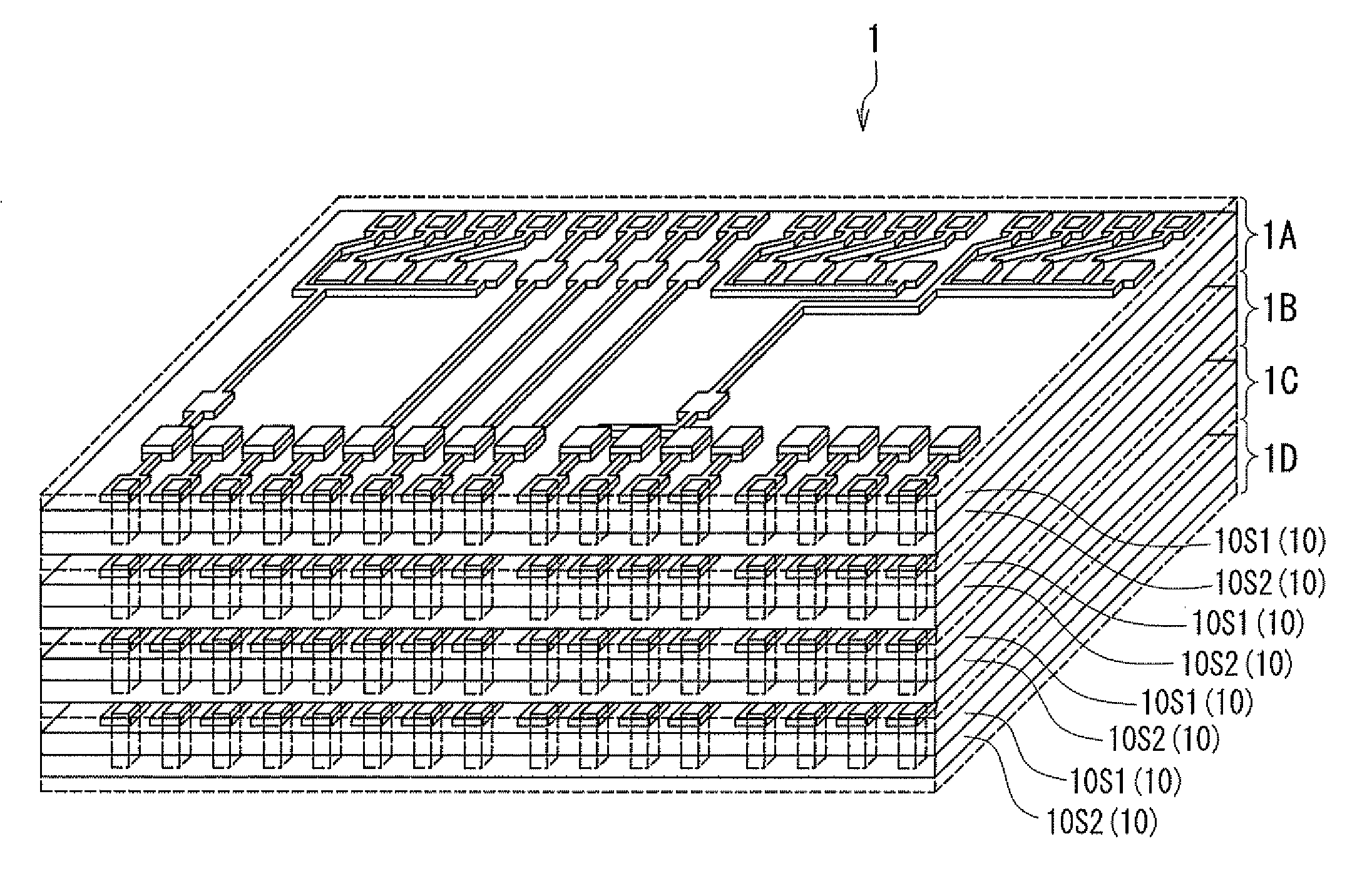
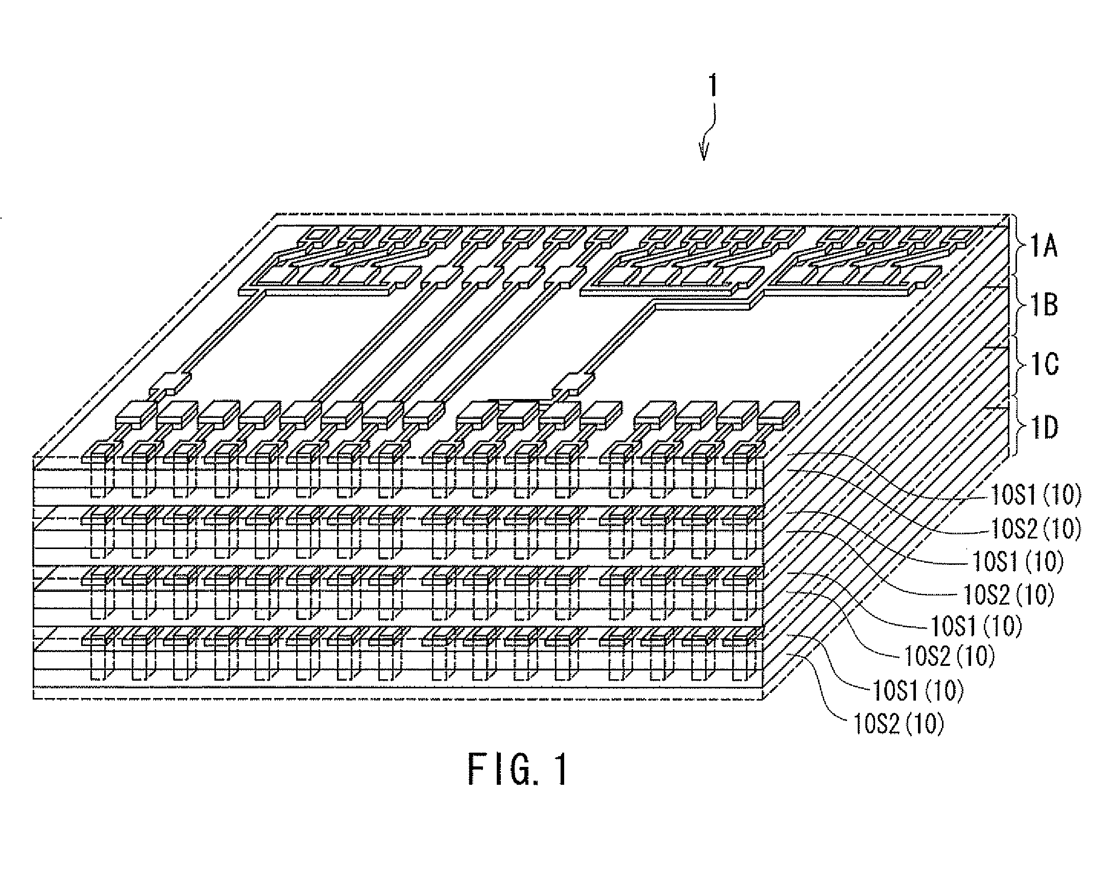
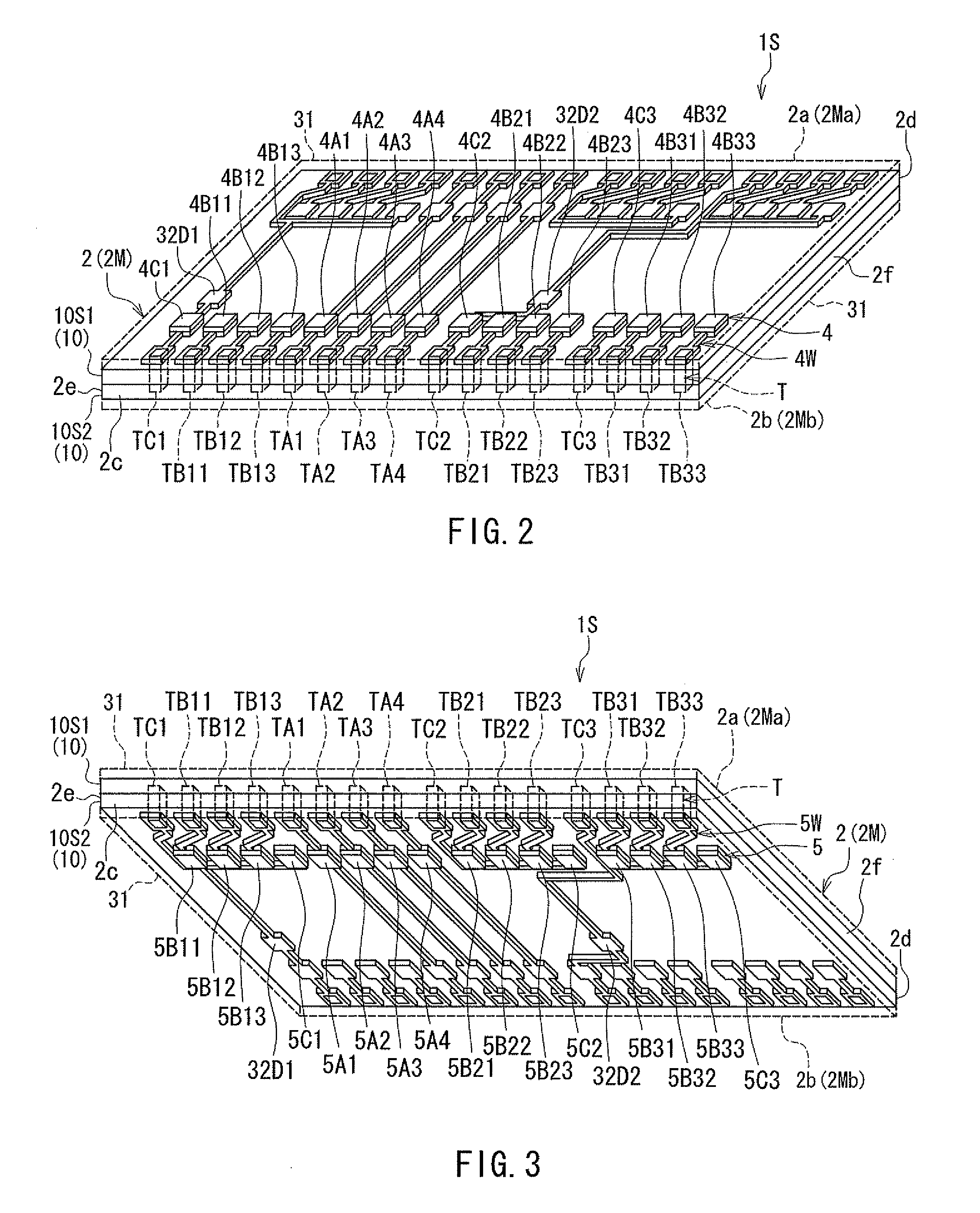
[0082]Preferred embodiments of the present invention will now be described in detail with reference to the drawings. First, reference is made to FIG. 1 to FIG. 5 to describe the configurations of a layered chip package and a composite layered chip package according to a first embodiment of the invention. FIG. 1 is a perspective view of the composite layered chip package according to the present embodiment. FIG. 2 is a perspective view of the layered chip package according to the present embodiment. FIG. 3 is a perspective view showing the layered chip package of FIG. 2 as viewed from below. FIG. 4 is a plan view showing a layer portion included in the layered chip package of FIG. 2. FIG. 5 is a perspective view of the layer portion shown in FIG. 4.

[0083]As shown in FIG. 1, the composite layered chip package 1 according to the present embodiment includes a plurality of subpackages stacked, every two vertically adjacent subpackages being electrically connected to each other. FIG. 1 sh...

second embodiment

[0228]A second embodiment of the invention will now be described. In the method of manufacturing a layered chip package according to the present embodiment, the step of fabricating the layered substructure is different from that of the first embodiment. The steps of the method of manufacturing the layered chip package according to the present embodiment are the same as those of the first embodiment up to the step shown in FIG. 19. Then, in the present embodiment, a plurality of openings for exposing the plurality of electrode pads 38 are formed in the insulating film 106P in the normally functioning pre-semiconductor-chip portions 30P, as in the first embodiment. At this time, in the present embodiment, a plurality of holes for accommodating a plurality of conductor parts are also formed in the insulating film 106P at the positions of the grooves 104P. The plurality of conductor parts are intended to form the plurality of through electrodes T.

[0229]Reference is now made to FIG. 42 a...


PUM


Abstract

A layered chip package includes a main body. The main body includes a main part, and further includes first terminals and second terminals disposed on the top and bottom surfaces of the main part, respectively. The main part includes first and second layer portions, and through electrodes penetrating them. The through electrodes are electrically connected to the first and second terminals. Each of the layer portions includes a semiconductor chip having a first surface and a second surface opposite thereto, and further includes surface electrodes. The surface electrodes are disposed on a side of the semiconductor chip opposite to the second surface. The first and second layer portions are bonded to each other such that the respective second surfaces face each other. The first terminals are formed by using the surface electrodes of the first layer portion. The second terminals are formed by using the surface electrodes of the second layer portion.

Description

BACKGROUND OF THE INVENTION[0001]1. Field of the Invention[0002]The present invention relates to a layered chip package that includes a plurality of semiconductor chips stacked, and to a method of manufacturing the same.[0003]2. Description of the Related Art[0004]In recent years, lighter weight and higher performance have been demanded of portable devices typified by cellular phones and notebook personal computers. Accordingly, there has been a need for higher integration of electronic components for use in the portable devices. With the development of image- and video-related equipment such as digital cameras and video recorders, semiconductor memories of larger capacity and higher integration have also been demanded.[0005]As an example of highly integrated electronic components, a system-in-package (hereinafter referred to as SiP), especially an SiP utilizing a three-dimensional packaging technology for stacking a plurality of semiconductor chips, has attracting attention in rece...

Claims


Application Information

Patent Timeline
IPC IPC(8): H01L23/48H01L21/50
CPCH01L24/92H01L24/96H01L2924/00014H01L2924/07802H01L2224/03009H01L2225/06565H01L2225/06541H01L2225/06558H01L2924/1434H01L25/0657H01L25/105H01L25/50H01L2924/3511H01L2224/05569H01L2224/05011H01L2224/05012H01L2224/037H01L22/22H01L24/03H01L24/05H01L24/13H01L24/16H01L2224/0362H01L2224/0401H01L2224/04105H01L2224/05008H01L2224/05147H01L2224/05644H01L2224/13144H01L2224/16145H01L2224/9202H01L2224/96H01L2225/1058H01L2224/03H01L2924/0105H01L2924/00H01L2224/05552H01L2924/181
Inventor SASAKI, YOSHITAKAITO, HIROYUKIIKEJIMA, HIROSHIIIJIMA, ATSUSHI
Owner HEADWAY TECH INC
Features
  • R&D
  • Intellectual Property
  • Life Sciences
  • Materials
  • Tech Scout
  • Unparalleled Data Quality
  • Higher Quality Content
  • 60% Fewer Hallucinations
Learn More