
Eureka
For R&D, Eureka makes reading and utilizing patents & technical documents easy.
Eureka AIR
Designed for self-driven R&D workflows. Generate viable solutions, solve complex R&D challenges, empower your innovation with AI.

Eureka Materials
Designed for material experts only. Revolutionize your material R&D, from search, analyze, to developing new materials.

TechResearch
Generate reliable direction feasibility study reports for your R&D in just a few steps.

TechSeek
Discover and master advanced knowledge NOW. Basics, ideas, possibilities, all at once.

TechMind
As an expert in R&D Theories, TechMind can generates customized viable solutions instantly.

TechRisk
Analyze your overall solution with one click, know your potential R&D risks in advance.

TechMonitor
Get weekly tech updates, stay abreast of the latest tech innovations and key insights.
Method of making a micro-electro-mechanical-systems (MEMS) device
- Summary
- Abstract
- Description
- Claims
- Application Information
AI Technical Summary
Problems solved by technology
Method used
Image

Examples
Embodiment Construction
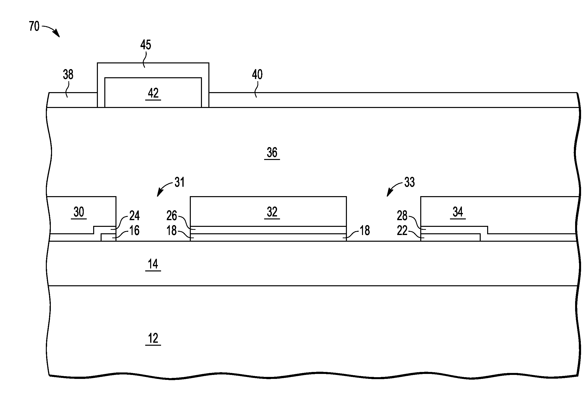
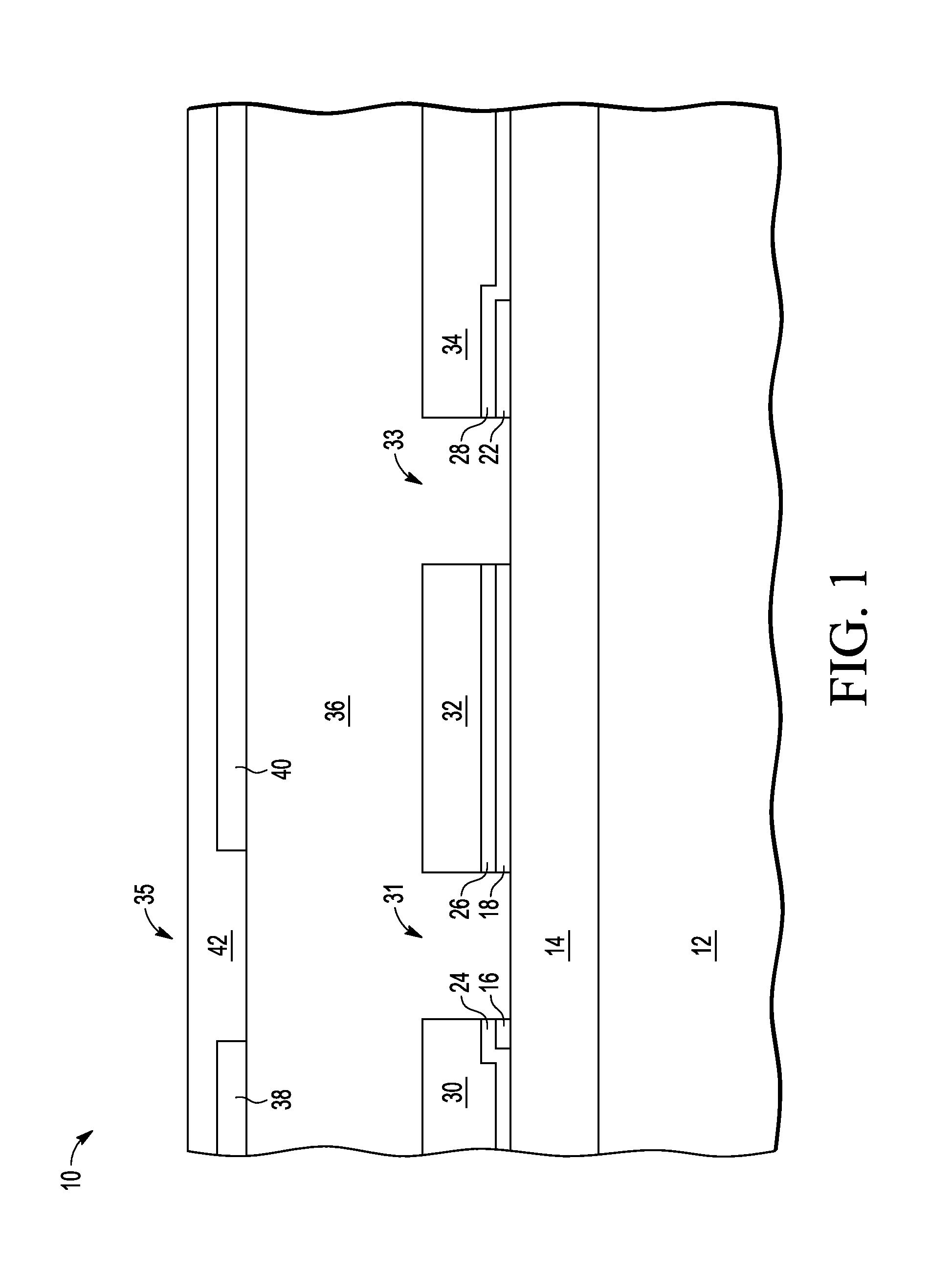
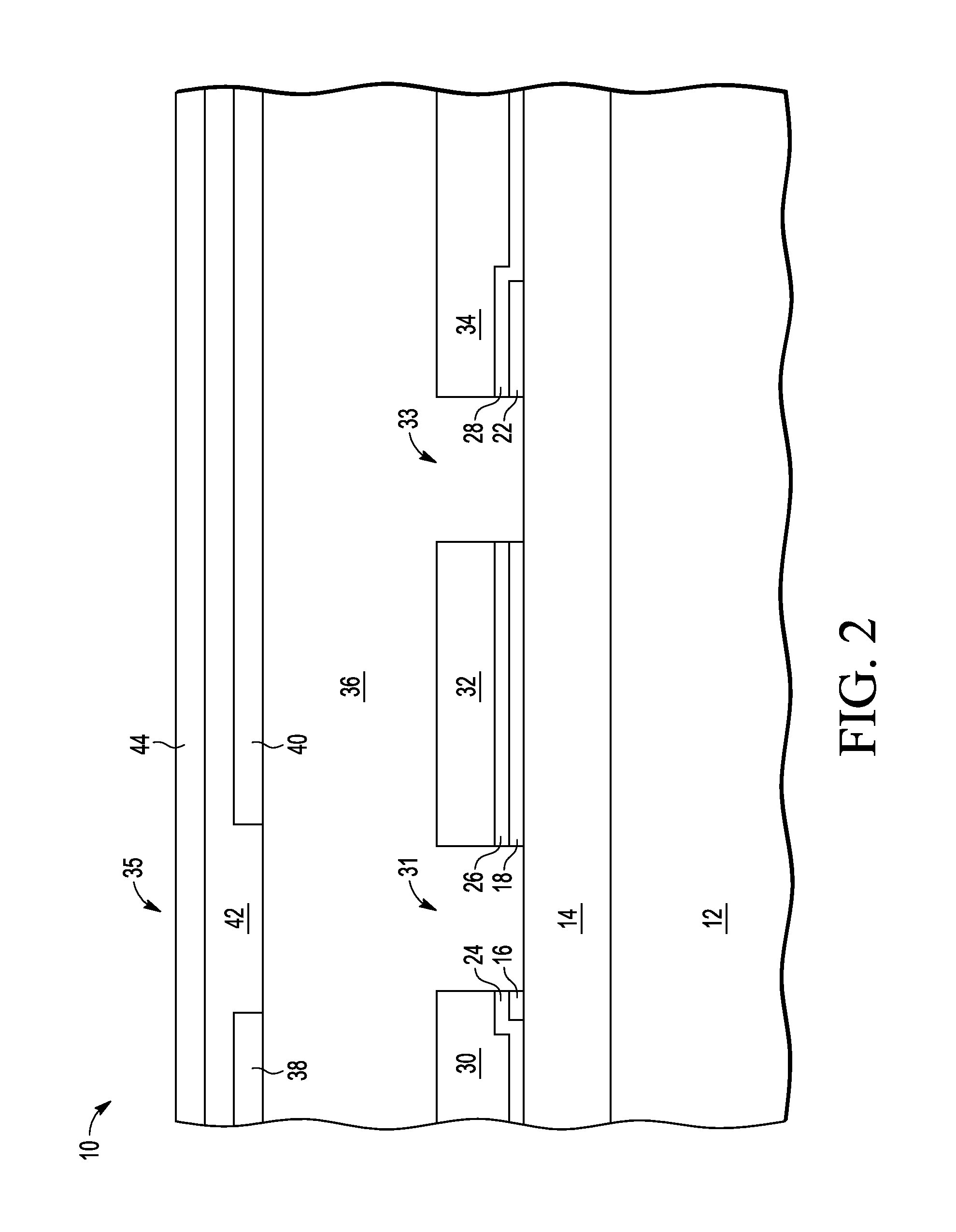
[0018]In one aspect, a micro-electro-mechanical-systems (MEMS) device is made using an etch that provides freedom of motion of a polysilicon member while protecting a contact pad from the etchants used to perform the etch that provides the freedom of motion. The protection is achieved by depositing a sacrificial layer and patterning it to leave a portion over the location of the contact pad. The etch tends to leave a layer on the contact pad, if it is unprotected, that makes it difficult to adhere a wire bond or other contacting material. The etch is very significant to the freedom of motion and thus is very important to control in order to achieve the needed performance of the MEMS device. The remaining portion of the sacrificial layer is removed after the etch to make the contact available for contacting. This is better understood by reference to the drawings and the following specification.
[0019]The semiconductor substrate described herein can be any semiconductor material or com...
PUM
 Abstract
Description
Claims
Application Information
 - R&D Engineer
- R&D Manager
- IP Professional
- Industry Leading Data Capabilities
- Powerful AI technology
- Patent DNA Extraction
Browse by: Latest US Patents, China's latest patents, Technical Efficacy Thesaurus, Application Domain, Technology Topic, Popular Technical Reports.
© 2024 PatSnap. All rights reserved.Legal|Privacy policy|Modern Slavery Act Transparency Statement|Sitemap|About US| Contact US: help@patsnap.com