Wafer level lens, production method of wafer level lens, and imaging unit

a production method and technology applied in the field of wafer level lens, can solve the problems of increasing the production cost corresponding to this process, affecting the quality of the lens, so as to prevent the generation of light transmission and reflection at a region other than the lens surface, and prevent the transmission of light

Inactive Publication Date: 2012-05-31
FUJIFILM CORP
View PDF3 Cites 55 Cited by
  • Summary
  • Abstract
  • Description
  • Claims
  • Application Information

AI Technical Summary

Benefits of technology

[0022]In a usual glass wafer, owing to reflection at the surface and reflection of a transmitted light in the glass wafer, reflection of 5 to 10% occurs corresponding to about 2 times of the surface reflection. In contrast, this wafer level lens has a light shielding layer and a low reflective light shielding layer. The light shielding layer has a function of preventing transmission of a light in a substrate, by reflecting a light incoming from the outside of the wafer level lens. When a plurality of substrates are disposed, a light incoming from the top substrate surface is reflected by the light shielding layer at a region other than the lens, and it is possible to prevent the light penetrated through a region other than the lens from penetrating between the substrates and to the sensor substrate side.
[0023]By providing the low reflective light shielding layer, transmission of a light at a region other than the lens surface of the lens can be prevented.
[0024]By providing both the light shielding layer and the low reflective light shielding layer, a light penetrating a part other than the lens can be reflected by the light shielding layer, and even if a light penetrates into the substrate without reflection by the light shielding layer, the light can be shielded by the low reflective light shielding layer. Accordingly, generation of light transmission and reflection at a region other than the lens surface of the lens can be prevented, and defects in optical performances such as ghosts and flares in taking an image can be suppressed.
[0025]Further, since the light shielding layer and the low reflective light shielding layer are patterned on the surface of the substrate, there is no necessity to attach another light shielding member and the like to the wafer level lens and an increase in the production cost can be suppressed.
[0026]The present invention is capable of providing a wafer level lens with which a sufficient light shielding property is obtained, generation of defects such as ghosts, flares and the like due to a reflected light can be prevented, and an increase in the production cost can be suppressed; a production method of a wafer level lens, and an imaging unit.

Problems solved by technology

Owing to this constitution, if a wafer level lens is diced and placed on an imaging device to give an imaging unit and when light transmission and reflection occur at a region other than the lens surface of the lens, there is a fear of tendency of defects in optical performances such as ghosts and flares in taking an image.
However, if a light shielding member is separately attached, an increase in the production cost corresponding to this process is inevitable.

Method used


Image

  • Wafer level lens, production method of wafer level lens, and imaging unit
  • Wafer level lens, production method of wafer level lens, and imaging unit
  • Wafer level lens, production method of wafer level lens, and imaging unit

Examples


Embodiment Construction

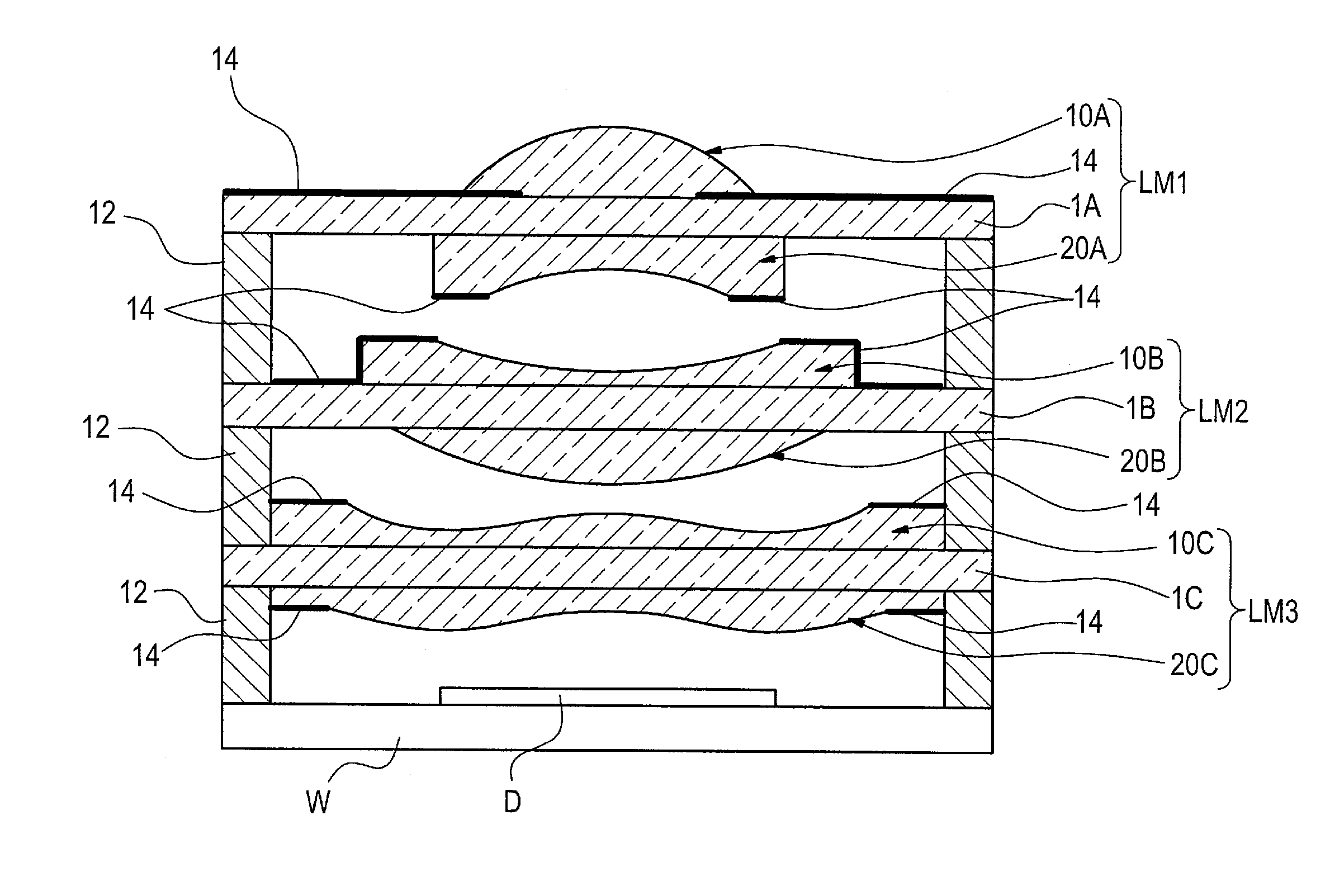
[0041]First, the constitutions of a wafer level lens and an imaging unit will be explained.

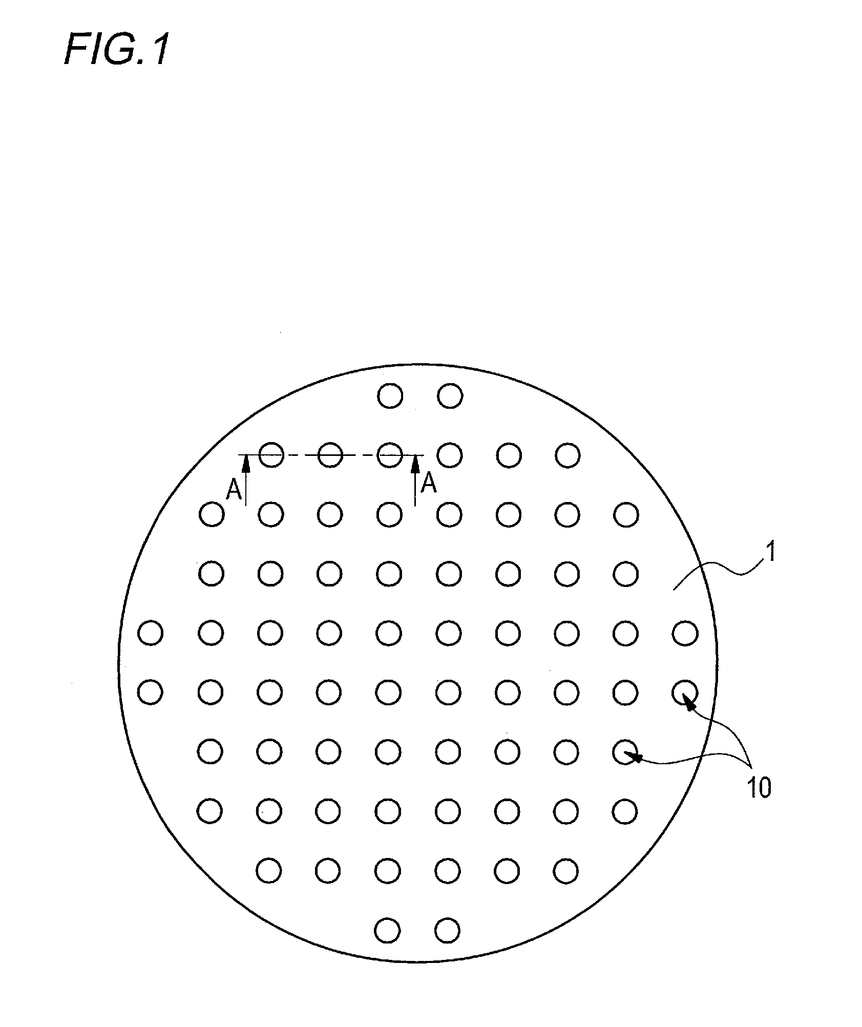
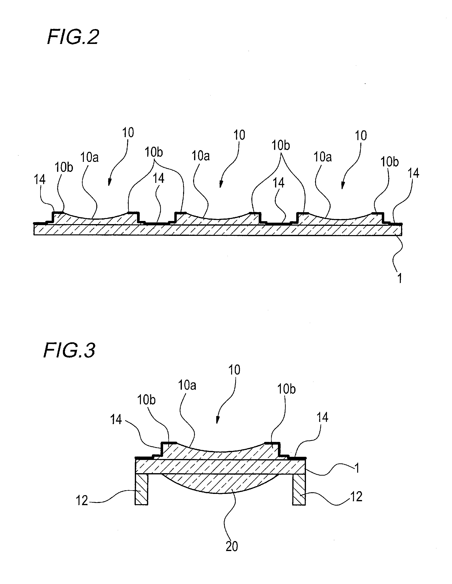
[0042]FIG. 1 is a plane view showing one example of the constitution of a wafer level lens. FIG. 2 is a cross-sectional view taken in a line A-A of the constitution of the wafer level lens shown in FIG. 1.

[0043]The wafer level lens has a lens module having a substrate 1 and a plurality of lenses 10 formed on the substrate 1. The plurality of lenses 10 are arranged on the substrate 1 in one-dimensional mode or two-dimensional mode. In this constitution example, an example of a constitution in which the plurality of lenses 10 are arranged on the substrate 1 in two-dimensional mode as in FIG. 1 will be explained. The lens 10 is constituted of the same material as for the substrate 1, and molded on the substrate 1.

[0044]As shown in FIG. 2, the lens 10 has a concave-shaped lens surface 10a and a lens marginal part 10b around the lens surface 10a. Here, the lens surface 10a has an optical property o...


PUM

PropertyMeasurementUnit
transmittanceaaaaaaaaaa

Abstract

A sufficient light-shielding property is obtained by a wafer level lens having at least one lens module having a substrate and a plurality of lenses formed on the substrate in which the wafer level lens has a black resist layer formed on the surface of the lens module or on the surface of the substrate and the black resist layer is formed with a pattern having an opening at a part intersecting the optical axis of the lens, and generation of defects such as ghosts, flares and the like due to a reflected light can be prevented and an increase in the production cost can be suppressed.

Description

TECHNICAL FIELD[0001]The present invention relates to a wafer level lens, a production method of a wafer level lens, and an imaging unit.BACKGROUND ART[0002]Presently, a portable terminal of electronic instruments such as cellular phones, PDAs (Personal Digital Assistants) and the like is loaded with a small and thin imaging unit. Such an imaging unit is generally equipped with a solid state imaging device such as a CCD (Charge Coupled Device) image sensor, a CMOS (Complementary Metal-Oxide Semiconductor) image sensor and the like, and a lens for forming a subject image on the solid state imaging device.[0003]With reduction in size and thickness of a portable terminal, reduction in size and thickness of an imaging unit is requested. For lowering the cost of a portable terminal, an efficient production process is desired. As the method of producing a lot of such small lenses, there is known a method in which a wafer level lens having a constitution containing a plurality of lenses mo...

Claims


Application Information

Patent Timeline
Patent Type & Authority Applications(United States)
IPC IPC(8): G02B7/02B05D5/06
CPCG02B3/0031G02B7/022G02B13/001H01L27/14627G02B1/11G02B13/0085B29D11/00009B29D11/00307B29D11/00G02B13/18H01L27/146H04N23/00
Inventor MARUYAMA, YOICHI
Owner FUJIFILM CORP
Why Eureka
Try Eureka