Method of fabricating a microcircuit device

a micro-circuit and electronic device technology, applied in the direction of semiconductor devices, instruments, computing, etc., can solve the problems of inability to withstand inability to carry the micro-circuit carried by the module, and inability to adapt to significant bending of the module, etc., to achieve the effect of improving the ability to withstand card strength tests, simple implementation, and reliable card

Active Publication Date: 2012-06-07
IDEMIA FRANCE
View PDF3 Cites 18 Cited by
  • Summary
  • Abstract
  • Description
  • Claims
  • Application Information

AI Technical Summary

Benefits of technology

[0008]A particular object of the invention is to remedy that drawback by proposing a method of fabricating a smart card, in particular one made of fibrous material such as paper or card, enabling the reliability of the card and its ability to withstand card strength tests to be improved, while also being very simple to implement.

Problems solved by technology

Nevertheless, the use of cards made of paper presents certain drawbacks.
While performing such tests on paper cards, it has been found that the force to which the card is subjected is sufficient for the paper to be flattened so that it cannot accommodate significant bending of the module.
Unfortunately, when the bending of the module becomes too great, the microcircuit carried by the module is liable to become damaged, or even to be made inoperative.
As a result, after performing such tests, a large number of microcircuit cards are considered to be faulty and end up being rejected during fabrication, which represents a non-negligible expense.

Method used


Image

  • Method of fabricating a microcircuit device
  • Method of fabricating a microcircuit device
  • Method of fabricating a microcircuit device

Examples


Embodiment Construction

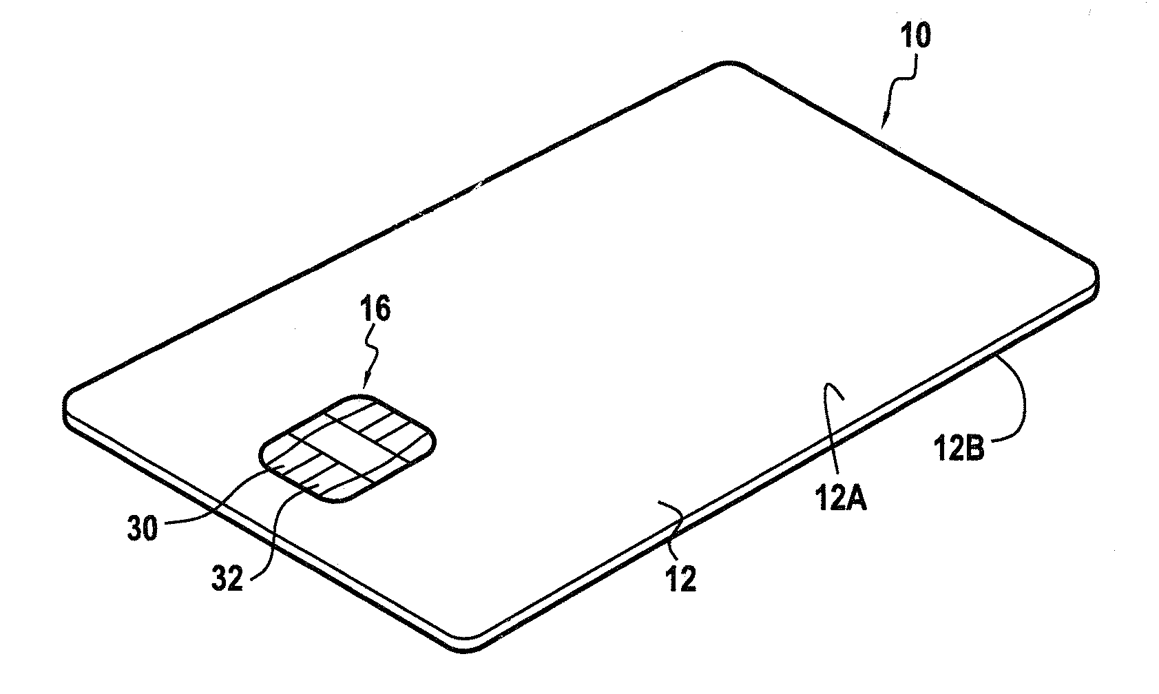
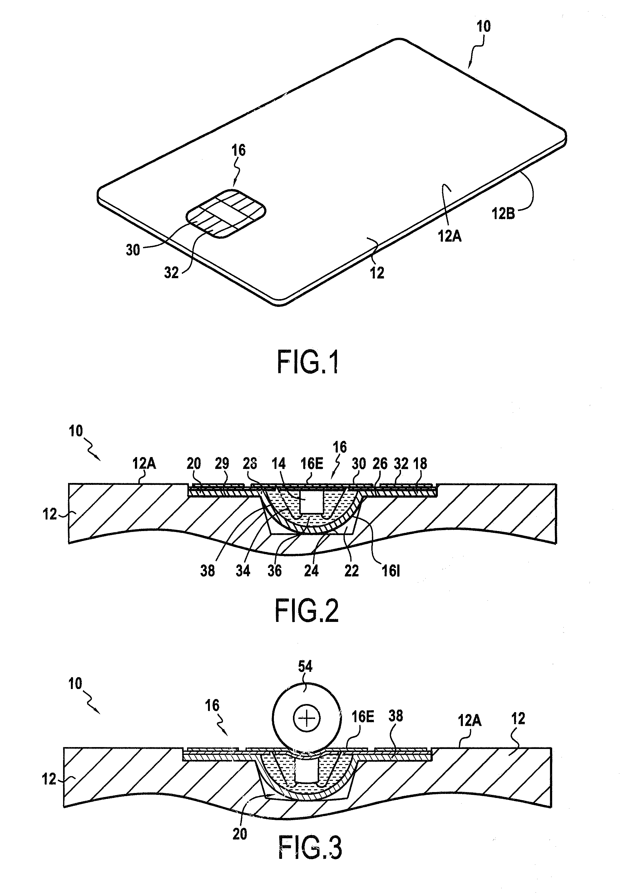
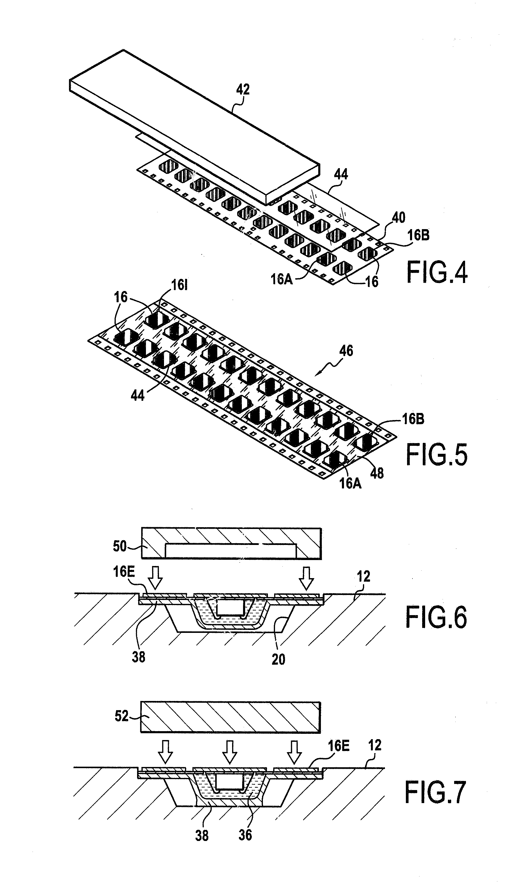
[0028]FIG. 1 shows a microcircuit device of the invention. This device is given overall reference 10.

[0029]In the example described, the microcircuit device 10 is a smart card. In a variant, the device 10 could be a page of a passport such as the cover of the passport, or indeed it could be an adhesive label or “sticker”.

[0030]As shown in FIG. 1, the device 10 comprises a body 12 that is generally card-shaped, defining first and second opposite faces 12A and 12B.

[0031]In this embodiment, the body 12 defines the outside dimensions of the card 10. In this example, and preferably, the dimensions of the card 10 are defined by the ID-1 format of the ISO 7816 standard, which is the format conventionally used for bank cards, having dimensions of 85.6 millimeters (mm) by 53.98 mm and thickness that is substantially equal to eight hundred micrometers. Naturally, other card formats could also be used.

[0032]The card body 12 is preferably made of a fibrous material, e.g. based on natural and / or...


PUM

PropertyMeasurementUnit
thicknessaaaaaaaaaa
thicknessaaaaaaaaaa
thicknessaaaaaaaaaa

Abstract

A fabrication method for a device having a body having a cavity of dimensions suitable for receiving a module having a microcircuit, the cavity having a bottom and a peripheral wall surrounding the bottom, the method including a step of putting the module into place in the cavity. More precisely, the method comprises, prior to the step of putting the module into place, a step of depositing an adhesive strip at least on a surface of the module that is designed to face the bottom of the cavity, the adhesive strip being suitable for enabling the module to adhere at least to the bottom of the cavity and for limiting a deformation stroke of the module that could occur under the effect of a mechanical compression force urging the module against the bottom of the cavity.

Description

FIELD OF THE INVENTION[0001]The present invention relates to the technical field of portable microcircuit electronic devices, such as in particular smart cards.[0002]The invention applies more particularly but not exclusively to contact type microcircuit cards, also known more generally as smart cards, of format in compliance with the ID-1 format defined by the ISO-7816 standard.BACKGROUND OF THE INVENTION[0003]Such a smart card generally comprises a body made of plastics material and provided with a cavity for receiving a microcircuit module, the module being fastened to the body, e.g. by adhesive.[0004]At present, there exists a need to make cards, in particular smart cards, out of paper or card material. Such a material presents numerous advantages: firstly it is recyclable or indeed biodegradable, and secondly its cost is generally less than the cost of conventional plastics such as polyvinylchloride (PVC) or PVC acryolonitrile-butadiene-styrene (ABS) copolymer, as are con...

Claims


Application Information

Patent Timeline
Patent Type & Authority Applications(United States)
IPC IPC(8): G06K19/077B29C65/02
CPCG06K19/07745H01L2224/48091H01L2224/48227H01L2224/45144H01L2924/00014H01L2924/00
Inventor BOSQUET, OLIVIERBOSCHET, JEAN-FRANCOIS
Owner IDEMIA FRANCE
Why Eureka
Try Eureka