Organic light-emitting display apparatus and method of manufacturing the same

a technology of light-emitting display and organic materials, which is applied in the direction of electrical equipment, basic electric elements, semiconductor devices, etc., can solve the problems of lifting phenomenon and increase in the cost of fabricating masks, and achieve the effect of reducing the number of patterning process using masks

Active Publication Date: 2012-06-07
SAMSUNG DISPLAY CO LTD
View PDF6 Cites 39 Cited by
  • Summary
  • Abstract
  • Description
  • Claims
  • Application Information

AI Technical Summary

Benefits of technology

[0010]The present invention provides an organic light-emitting display apparatus and a method of manufacturing the same by which the number of processes of patterning using a mask can be reduced and an organic layer coating defect problem in a pad region can be solved.

Problems solved by technology

In the process of transferring a pattern by using the mask, as described above, it is necessary to prepare the mask having a required pattern, and thus the cost of fabricating the mask increases as more operations are performed using the mask.
In this scheme, however, stress on the thick organic layer increases so that coating is not performed appropriately, especially in a pad region which is an end portion of the organic layer, resulting in a lifting phenomenon.

Method used


Image

  • Organic light-emitting display apparatus and method of manufacturing the same
  • Organic light-emitting display apparatus and method of manufacturing the same
  • Organic light-emitting display apparatus and method of manufacturing the same

Examples


Embodiment Construction

[0030]Hereinafter, an exemplary embodiment of the present invention will be described in detail with reference to the accompanying drawings.

[0031]Like reference numerals denote like elements throughout the specification. A detailed description of known functions and configurations will be omitted when it may unnecessarily obscure the subject matter of the present invention.

[0032]In the drawings for describing an embodiment of the present invention, the thicknesses of layers or regions are exaggerated for clarity. It will be understood that when an element such as a layer, film, region, or substrate is referred to as being “on” another element, it can be “directly on” the other element or intervening elements may also be present.

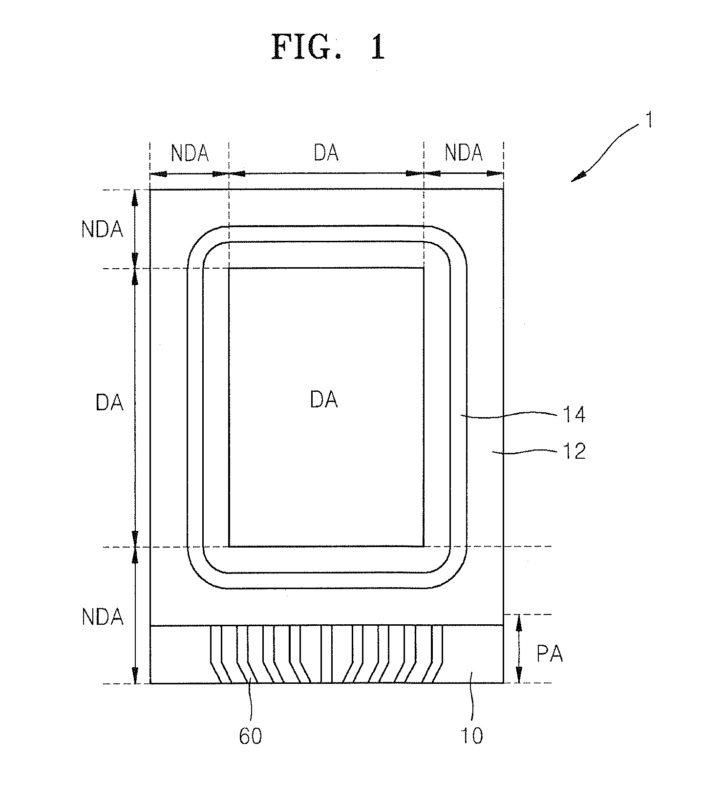
[0033]FIG. 1 is a plan view schematically showing a structure of an organic light-emitting display apparatus according to an exemplary embodiment of the present invention; and

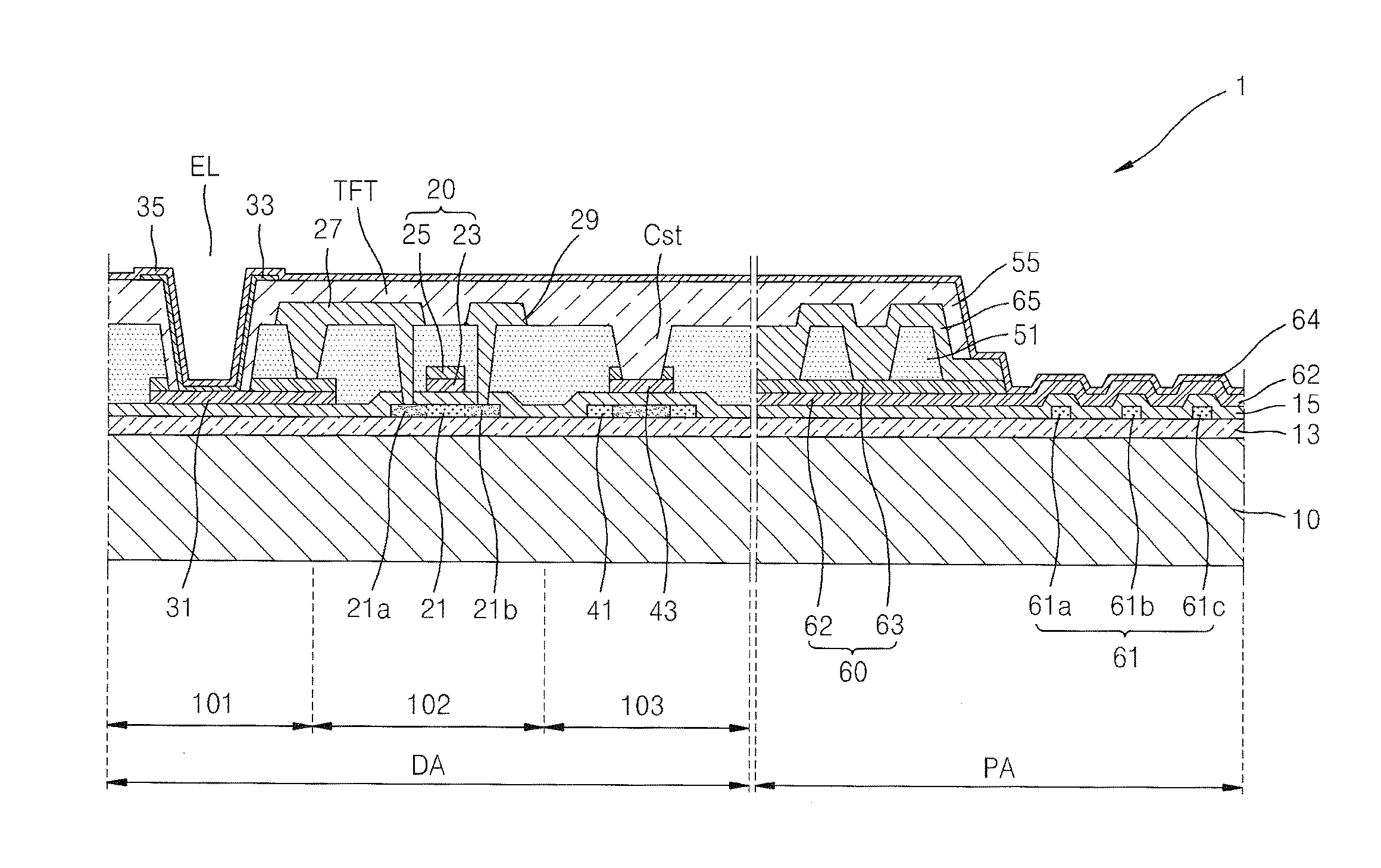
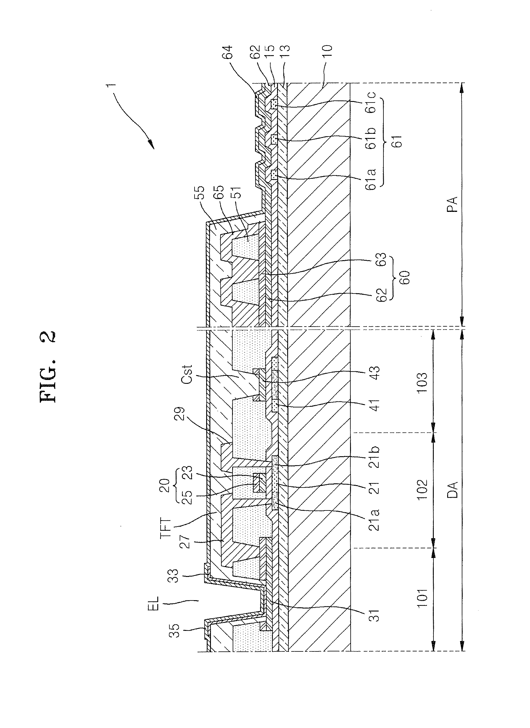
[0034]FIG. 2 is a cross-sectional view schematically showing a portion of the organi...


PUM


Abstract

In an organic light-emitting display apparatus and a method of manufacturing the same, a pad region of the organic light-emitting display apparatus comprises a protrusion layer including a plurality of protrusion portions formed on a substrate so as to protrude, a pad lower electrode and a pad upper electrode, the pad lower electrode including a protrusion portion formed along a protrusion outline of the protrusion layer and a flat portion formed along the substrate, and the pad upper electrode being formed on the flat portion of the pad lower electrode. A source / drain electrode layer is formed on the pad upper electrode, an organic layer is formed on the source / drain electrode layer, and a counter electrode layer is formed on the protrusion portion of the pad lower electrode and the organic layer. The counter electrode layer follows the protrusion outline of the protrusion layer on the protrusion portion. According to such a structure, cost is reduced due to a reduction in the number of masks, the manufacturing process is simplified, and a lifting phenomenon of the organic layer in the pad region is solved.

Description

CLAIM OF PRIORITY[0001]This application makes reference to, incorporates the same herein, and claims all benefits accruing under 35 U.S.C. §119 from an application earlier filed in the Korean Intellectual Property Office on 2 Dec. 2010 and there duly assigned Serial No. 10-2010-0122091.BACKGROUND OF THE INVENTION[0002]1. Field of the Invention[0003]The present invention relates to an organic light-emitting display apparatus and a method of manufacturing the same, and more particularly, to an organic light-emitting display apparatus and a method of manufacturing the same by which the number of mask uses can be reduced during manufacturing of the organic light-emitting display apparatus and a defect in coating an organic layer in a pad region can be corrected.[0004]2. Description of the Related Art[0005]An organic light-emitting display apparatus is manufactured on a substrate on which a pattern including a thin-film transistor (TFT), a capacitor, and wiring connecting the TFT and the...

Claims


Application Information

Patent Timeline
Patent Type & Authority Applications(United States)
IPC IPC(8): H01L27/32H01L51/56
CPCH01L27/3276H01L27/1255H01L29/4908H10K59/131H10K59/1216H10K59/1213H10K50/805
Inventor LEE, YUL-KYUYOU, CHUN-GIPARK, SUNPARK, JONG-HYUNKIM, KWANG-HAE
Owner SAMSUNG DISPLAY CO LTD
Why Eureka
Try Eureka