

Thermoelectric element and thermoelectric module including the same
a technology of thermoelectric modules and thermoelectric elements, applied in the direction of thermoelectric device details, thermoelectric device junction materials, electrical apparatus, etc., can solve the problems of increasing interest in a complex module using several single modules, and the entire complex module cannot operate, so as to improve the thermoelectric figure of merits
- Summary
- Abstract
- Description
- Claims
- Application Information
AI Technical Summary
Benefits of technology
Problems solved by technology
Method used
Image

Examples
example 1
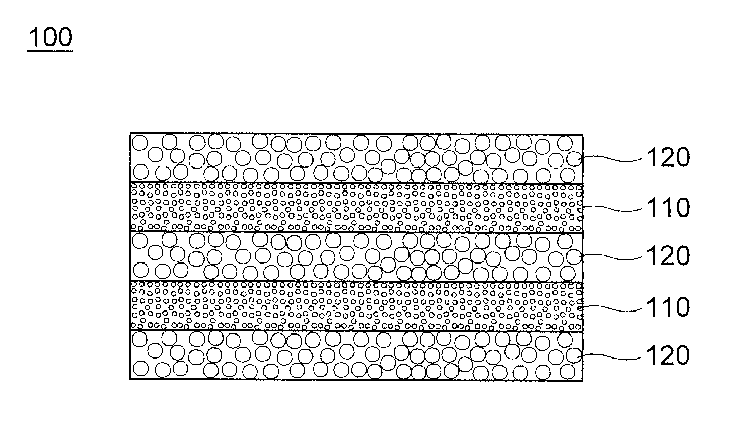
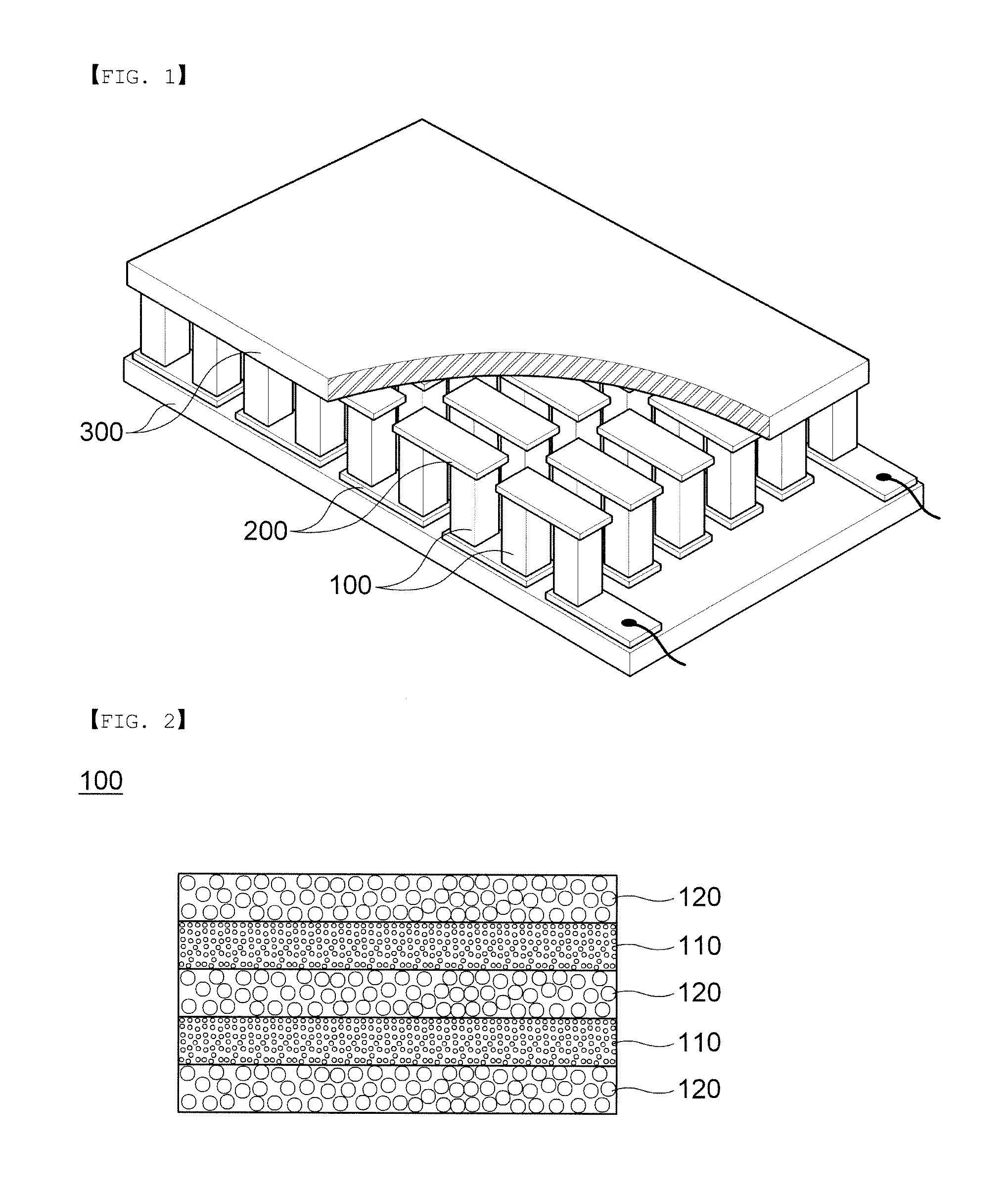
[0073]FIG. 2 shows a structure of a thermoelectric element 100 according to a first exemplary embodiment of the present invention.
[0074]Referring to FIG. 2, the thermoelectric element 100 may include: first semiconductor layers 110 formed of thermoelectric semiconductor materials; and second semiconductor layers 120 formed of semiconductor materials having a different diameter from the materials forming the first semiconductor layer 110.
[0075]At this time, the first semiconductor layers 110 and the second semiconductor layers 120 may be alternately laminated to maximize the difference of physical property at the interface between the layers. The first and second semiconductor layers may be laminated in three or more layers.
[0076]Also, it is preferable that the diameter of the materials forming the second semiconductor layers 120 is more than 5 times the diameter of the materials forming the first semiconductor layers 110, considering the interface effect due to the difference of phy...
example 2
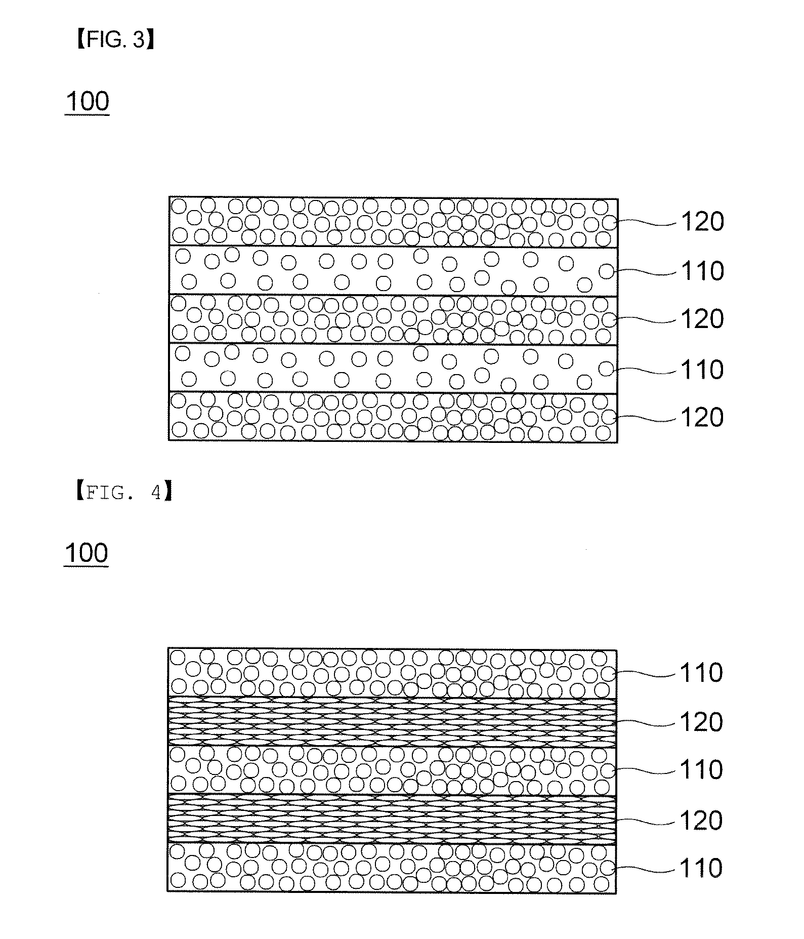
[0078]FIG. 3 shows a structure of a thermoelectric element 100 according to a second exemplary embodiment of the present invention.
[0079]Referring to FIG. 3, the thermoelectric element 100 may include: first semiconductor layers 110 formed of thermoelectric semiconductor materials; and second semiconductor layers 120 formed of semiconductor materials which make the second semiconductor layers 120 have a different density from the first semiconductor layers 110.
[0080]At this time, it is preferable that the density of the second semiconductor layers 120 is more than 1.5 times the density of the first semiconductor layers 110, in order to increase the scattering of phonons due to the interface effect between layers efficiently. If the difference of density is too small, the interface effect is not large such that the scattering of phonons is increased slightly, thereby making it impossible to accomplish the intended object.
[0081]Also, the first semiconductor layers 110 and the second s...
example 3
[0082]FIG. 4 shows a structure of a thermoelectric element 100 according to a third exemplary embodiment of the present invention.
[0083]Referring to FIG. 4, the thermoelectric element 100 may include: first semiconductor layers 110 formed of thermoelectric semiconductor materials; and second semiconductor layers 120 formed of thermoelectric semiconductor materials having a different flatness from the materials forming the first semiconductor layers 110.
[0084]The flatness may be numerically expressed by a ratio of major axis and minor axis of a particle.
[0085]In other words, if the minor axis / major axis ratio of the materials forming the first semiconductor layers 110 is different from the minor axis / major axis ratio of the materials forming the second semiconductor layers 120, the scattering of phonons can be increased at the interface between the two layers.
[0086]Herein, the rate of the minor axis / major axis ratio between the first semiconductor layers 110 and the second semiconduc...
PUM
 Abstract
Description
Claims
Application Information