Touch sensing output device

a technology of output device and touch sensor, which is applied in the direction of instruments, computing, electric digital data processing, etc., can solve the problems of reducing display brightness, wasting power, and reducing display brightness, so as to reduce manufacturing complexity and reduce the complexity of driving the system

Inactive Publication Date: 2012-06-14
KONINKLIJKE PHILIPS ELECTRONICS NV
View PDF5 Cites 68 Cited by
  • Summary
  • Abstract
  • Description
  • Claims
  • Application Information

AI Technical Summary

Benefits of technology

[0016]The invention is based on the recognition that suitably-designed electrodes can both drive the light transmission (i.e. display) effect as well as can be used for touch-input capacitance-sensing. Significant advantages are obtained in addition to the lack of additional layers being required, including reduced complexity in driving the system, and reduced manufacturing complexity.
[0020]The system of the invention gives an increase in display brightness compared to systems that require additional touch-sensor hardware overlying the display, and therefore a reduction in wasted power. Subsequent manufacturing advantages are permitted by the integration of the driving and sensing electrodes.

Problems solved by technology

The problem with the use of ITO electrodes is that even with their 95% transparency they reduce the display brightness, wasting power.
The problem with this technique is that it sacrifices pixel aperture in favor of the area demanded by the photodiode and its readout electrodes, reducing display brightness.
Touching the display results in its local deformation, and the consequent change in gap between bump and electrode leads to a change in capacitance and hence triggers a ‘touch’ event.
However, pixel aperture must be sacrificed for these ‘bumps’ and their capacitance-monitoring electrodes, leading once again to a reduction in display brightness and wasted power.

Method used


Image

  • Touch sensing output device
  • Touch sensing output device
  • Touch sensing output device

Examples


Embodiment Construction

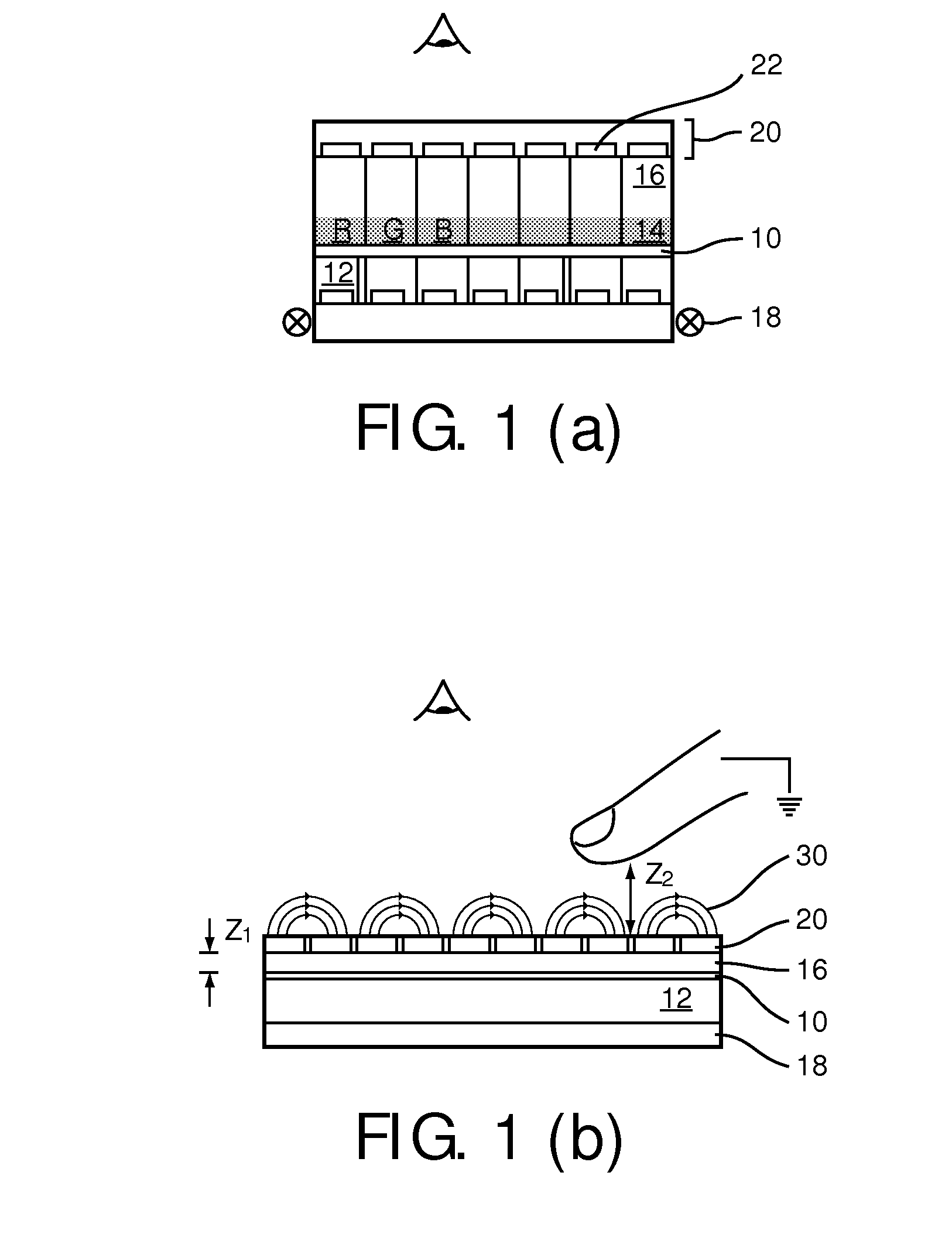
[0046]The invention will first be described in relation to a display device, although it will be apparent that the invention can be applied more generally to other devices which have variable light transmission characteristics.

[0047]In all common existing displays, particularly in liquid crystal (LC), organic light-emitting diode (OLED), and most existing electrophoretic display technologies, the requirement for separating the array of capacitance touch-measurement electrodes from the display front surface is a consequence of the continuous ground plane on their front surface.

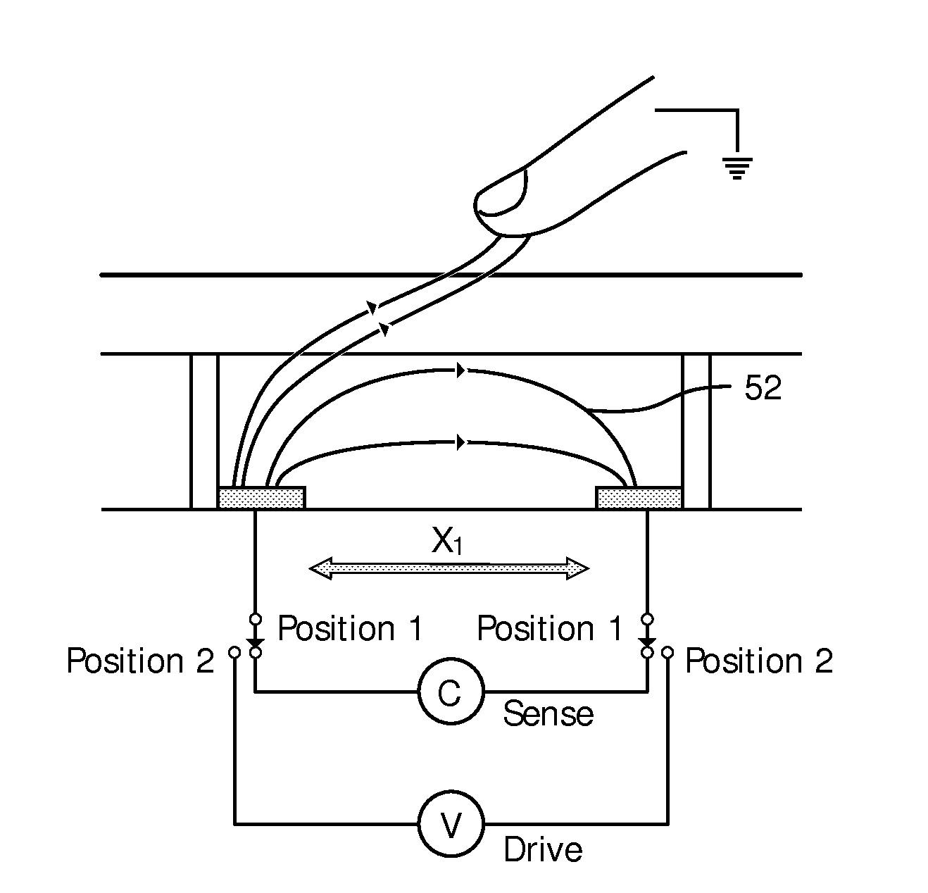
[0048]This is shown in FIG. 1. FIG. 1(a) is a cross section of a typical display that has a ground plane 10 overlying the LC cells 12. A color filter layer is shown as 14 and the coverglass is shown as 16. The light from a backlight 18 is modulated by the display pixels.

[0049]An attached capacitive-based touch-sensitive layer 20 is provided over the coverglass, and this uses additional transparent (ITO) electro...


PUM

PropertyMeasurementUnit
transparencyaaaaaaaaaa
thicknessaaaaaaaaaa
sizeaaaaaaaaaa

Abstract

A device having touch sensor input functionality, comprises first and second control electrodes (40,42) lying in a common plane. The device is operable in at least two modes, comprising: a first mode in which the light transmission characteristics are altered by controlling the movement of the charged particles under the influence of control signals applied to the first and second control electrodes; and a second mode in which the first and second control electrodes are coupled to a capacitance sensing means, for detecting a change in capacitance caused by the proximity of an object to be detected.

Description

FIELD OF THE INVENTION[0001]This invention relates to touch sensing output devices, for example touch sensing displays.BACKGROUND OF THE INVENTION[0002]The use of capacitance sensing as a means for detecting touch input is well known and the subject of much current development.[0003]Applications at the more advanced functionality end of the spectrum are typified by the high resolution capability offered by the Apple iPhone, and at the reduced functionality end lie simpler on-off touch sensors for operating electrical appliances such as lighting.[0004]At the heart of all these capacitance sensing systems is a detection system that measures a sense capacitor that is designed as the input ‘switch’. Each switch is designed as a flat conductive pad whose surface area corresponds to the sensed area for that particular switch. The value of this sense capacitor is designed so as to be dependent upon the proximity of a user's finger or an input stylus. As soon as the user's finger is suffici...

Claims


Application Information

Patent Timeline
Patent Type & Authority Applications(United States)
IPC IPC(8): G06F3/044G02F1/167G02F1/16761
CPCG02F1/167G06F3/044G06F3/0412G02F2001/1676G06F3/0445G06F3/0446G02F1/16761G02F1/1676G06F3/0416
Inventor FAIRLEY, PETER DOUGLASSIMONS, PAUL RICHARDPITCHERS, STEPHEN MICHAELVERSCHUEREN, ALWIN ROGIER MARTIJNVAN DELDEN, MARTINUS HERMANUS WILHELMUS MARIALENSSEN, KARS-MICHIELMULLER, MANFREDSTOFMEEL, LEON WILHELMUS GODEFRIDUS
Owner KONINKLIJKE PHILIPS ELECTRONICS NV
Why Eureka
Try Eureka