
Photoelectric conversion device

a conversion device and photoelectric technology, applied in the direction of photovoltaics, semiconductor devices, electrical equipment, etc., can solve the problems of the decrease in the amount of electric power generated, and achieve the effect of generating a large amount of electric power

Active Publication Date: 2012-06-21
SEMICON ENERGY LAB CO LTD
View PDF6 Cites 0 Cited by
  • Summary
  • Abstract
  • Description
  • Claims
  • Application Information

AI Technical Summary

Benefits of technology

[0017]According to one aspect of the present invention, incident light is divided by the light-dividing devices into a plurality of wavelength bands to fall onto the photoelectric conversion elements provided for the first to third substrates. Thus, a photoelectric conversion device can be provided which is capable of generating a large amount of electric power. In addition, the light-dividing devices serve as braces, and thus can distribute, to the third substrate, pressures and impacts applied to the first substrate or / and the second substrate, and distribute, to the first and second substrates, pressures and impacts applied to the third substrate. Therefore, a photoelectric conversion device can be provided which has resistance to pressures and impacts. Furthermore, these advantageous effects are effectively produced with the substantially U-shaped arrangement of the first to third substrates, and the area of the device can be thus prevented from being increased.
[0018]In addition, one aspect of the present invention is the photoelectric conversion device, wherein the first light-dividing device and the second light-dividing device have different wavelength bands for a reflectance of 80% or more in a wavelength hand of 350 nm or more and 2000 nm or less.
[0019]According to one aspect of the present invention, light can be prevented from being generated, which is reflected by both the first and second light-dividing devices to fail to reach the first to third photoelectric conversion elements. Therefore, a photoelectric conversion device can be provided which is capable of generating a large amount of electric power.
[0020]In addition, one aspect of the present invention is the photoelectric conversion device, wherein a protective substrate is provided in a region overlapped with the third substrate, and the protective substrate is secured to or near upper ends of the first substrate and the second substrate.
[0021]According to one aspect of the present invention, impacts applied to the first substrate or the second substrate can be distributed by the protective substrate to the opposite substrate. Therefore, a photoelectric conversion device can be provided which has resistance to pressures and impacts. In addition, the protective substrate can protect the light-dividing devices and the photoelectric conversion elements from impacts due to blown-off objects. Therefore, a photoelectric conversion device can be provided which is capable of generating a large amount of electric power over a long period of time.
[0022]In addition, one aspect of the present invention is a photoelectric conversion device, wherein the first substrate and the second substrate of the photoelectric conversion device configured as described above have end surfaces secured to portions of adjacent photoelectric conversion devices.

Problems solved by technology

For this reason, light loss such as light absorption or reflection by the upper photoelectric conversion layer is caused, and the incident light is thus diminished in the lower photoelectric conversion layer, which results in a decrease in the amount of electric power generated.

Method used


Image

  • Photoelectric conversion device
  • Photoelectric conversion device
  • Photoelectric conversion device

Examples


embodiment 1

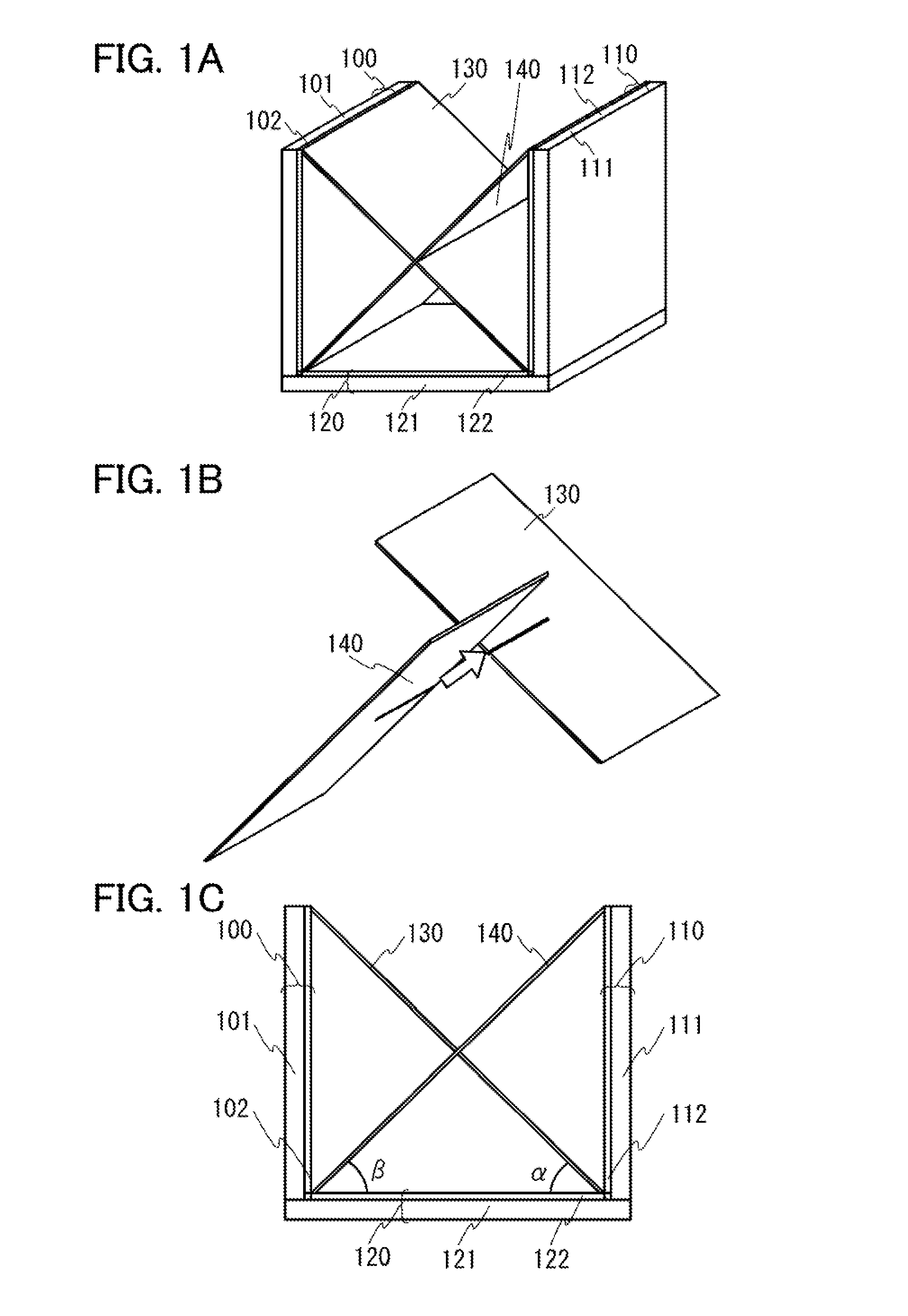
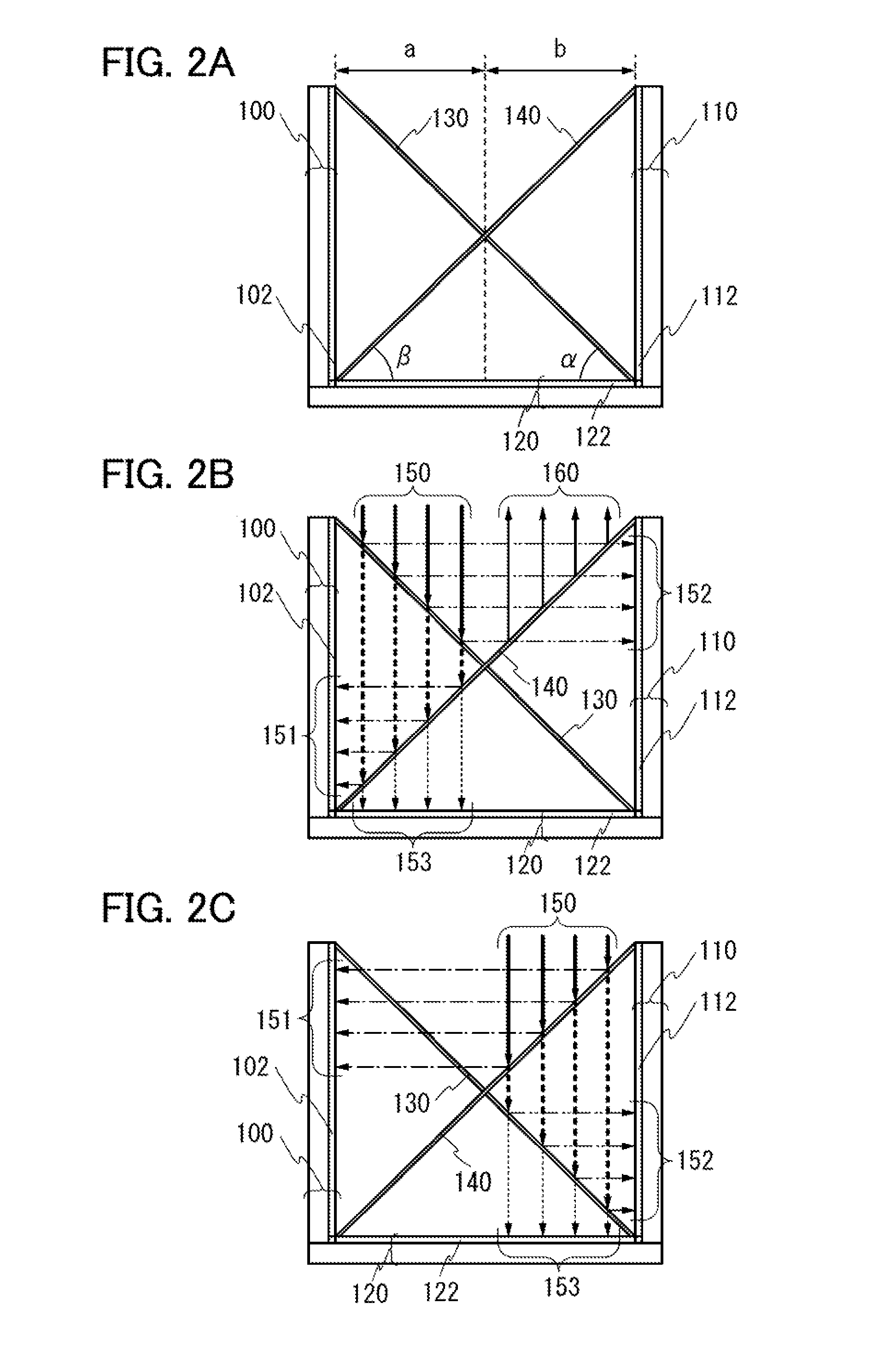
[0044]In the present embodiment, a photoelectric conversion device according to an aspect of the invention to be disclosed will be described with reference to FIGS. 1A to 1C, FIGS. 2A to 2C, and FIGS. 3A to 3C.

[0045]FIGS. 1A to 1C show structure diagrams of a photoelectric conversion device in the present embodiment. FIG. 1A is a perspective view of the photoelectric conversion device in the present embodiment, FIG. 1B is a diagram selectively illustrating a section of the structure in FIG. 1A, and FIG. 1C is a side view of FIG. 1A.

[0046]The photoelectric conversion device according to the present embodiment has, as shown in FIG. 1A, a first substrate 100 including a first base substrate 101 and a first photoelectric conversion element 102, a second substrate 110 including a second base substrate 111 and a second photoelectric conversion element 112, and a third substrate 120 including a third base substrate 121 and a third photoelectric conversion element 122, which are arranged in...

embodiment 2

[0097]In the present embodiment, a function will be described with reference to FIGS. 4A and 4B, which is different from that of the photoelectric conversion device according to one aspect of the present invention as described in Embodiment 1.

[0098]FIG. 4A is a side view of the same photoelectric conversion device as in FIG. 2A. The photoelectric conversion device described in the present embodiment has a structure as shown in FIG. 4A, in which a first hollow section 510 surrounded by the first substrate 100, the first light-dividing device 130, and the second light-dividing device 140, a second hollow section 520 surrounded by the second substrate 110, the first light-dividing device 130, and the second light-dividing device 140, and a third hollow section 530 surrounded by the third substrate 120 the first light-dividing device 130, and the second light-dividing device 140 are formed by securing the fixing portions (circular sections of dotted lines in FIG. 4A) of the substrates a...

embodiment 3

[0105]In the present embodiment, a photoelectric conversion device will be described with reference to FIGS. 5A to 5C and FIGS. 6A and 6B, which includes the plurality of photoelectric conversion devices described in the embodiments above.

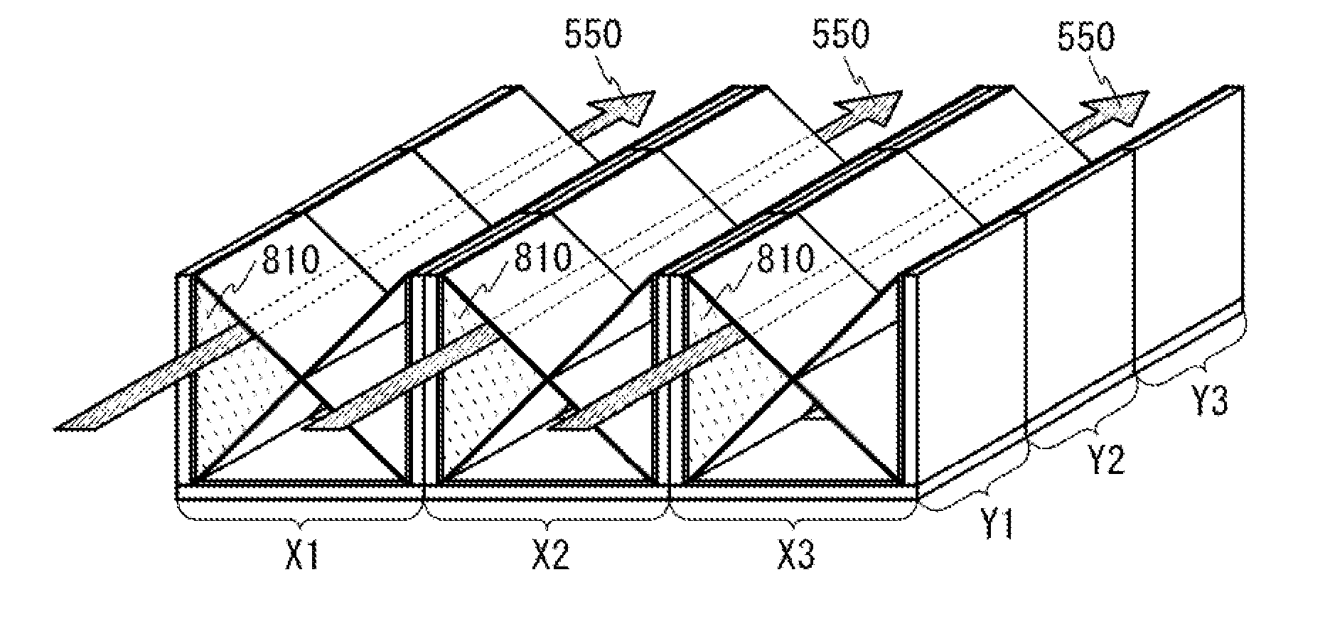
[0106]It is to be noted that when one photoelectric conversion device is to be specified among the plurality of placed photoelectric conversion devices, the device is represented by using coordinates in FIGS. 5A to 5C and FIGS. 6A and 6B. For example, the photoelectric conversion device placed in the center of FIG. 5A is represented as the “photoelectric conversion device in the range of X2 and Y2”, and the three photoelectric conversion devices placed in the front in FIG. 5A are represented as the “photoelectric conversion devices in the range of X1-X2-X3 and Y1”.

[0107]FIG. 5A is a diagram illustrating a photoelectric conversion device in which a plurality of photoelectric conversion devices with the structure of FIG. 1A as described in Embodiment...


PUM


Abstract

The present invention provides a photoelectric conversion device. Specifically, the photoelectric conversion device has a structure in which a substrate including a photoelectric conversion element provided at the bottom and a substrate including a photoelectric conversion element provided at the side are secured in a brace form by a light-dividing device. This structure divides incident light using the light-dividing device into a plurality of wavelength bands, and causes the divided light to fall onto the photoelectric conversion elements provided at the bottom and side, thereby making it possible to provide a photoelectric conversion device which is capable of generating a lame amount of electric power. In addition, the light-dividing device distributes pressures and impacts applied to the substrates at the bottom and side, thus making it possible to provide a photoelectric conversion device which has resistance to pressures and impacts.

Description

BACKGROUND OF THE INVENTION[0001]1. Field of the Invention[0002]The present invention relates to a photoelectric conversion device.[0003]2. Description of the Related Art[0004]In recent years, solar cells which generate electric power without carbon dioxide emissions have been attracting attention from the point of view of global warming prevention. Recently, the Japanese government has started subsidies for solar cells, and moreover, solar cells themselves have come to be less expensive. Thus, solar cells have been in widespread use not only in large-scaled solar power generation facilities but also in standard houses, e.g., on roofs of or outside the houses for power generation.[0005]Therefore, a variety of methods have been suggested in order to increase the amount of electric power to be generated by solar cells. As one of the methods, photoelectric conversion devices have been developed which are achieved by stacking layers for converting incident light into electrical energy (...

Claims


Application Information

Patent Timeline
Patent Type & Authority Applications(United States)
IPC IPC(8): H01L31/052
CPCH01L31/0549Y02E10/52H01L31/0232H01L31/054H02S40/00H02S40/20H02S40/22Y02E10/50
Inventor TANAKA, KOICHIROARITA, YU
Owner SEMICON ENERGY LAB CO LTD
Learn More