Method for manufacturing a strained channel mos transistor

Active Publication Date: 2012-06-21
STMICROELECTRONICS (GRENOBLE 2) SAS +1
View PDF4 Cites 0 Cited by
  • Summary
  • Abstract
  • Description
  • Claims
  • Application Information

AI Technical Summary

Benefits of technology

[0010]An embodiment provides a relatively simple method for forming strained-channel MOS transistors, which implies but few additional steps with respect to known methods.

Problems solved by technology

However, known methods are generally relatively complex to implement and necessitate a significant number of additional manufacturing steps with respect to conventional MOS transistor manufacturing methods.

Method used


Image

  • Method for manufacturing a strained channel mos transistor
  • Method for manufacturing a strained channel mos transistor
  • Method for manufacturing a strained channel mos transistor

Examples


Embodiment Construction

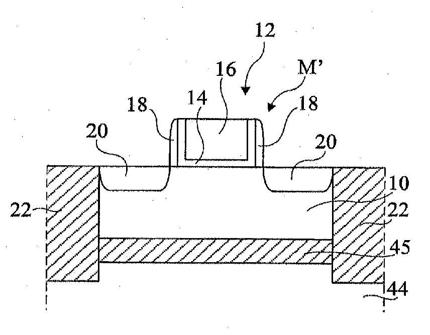
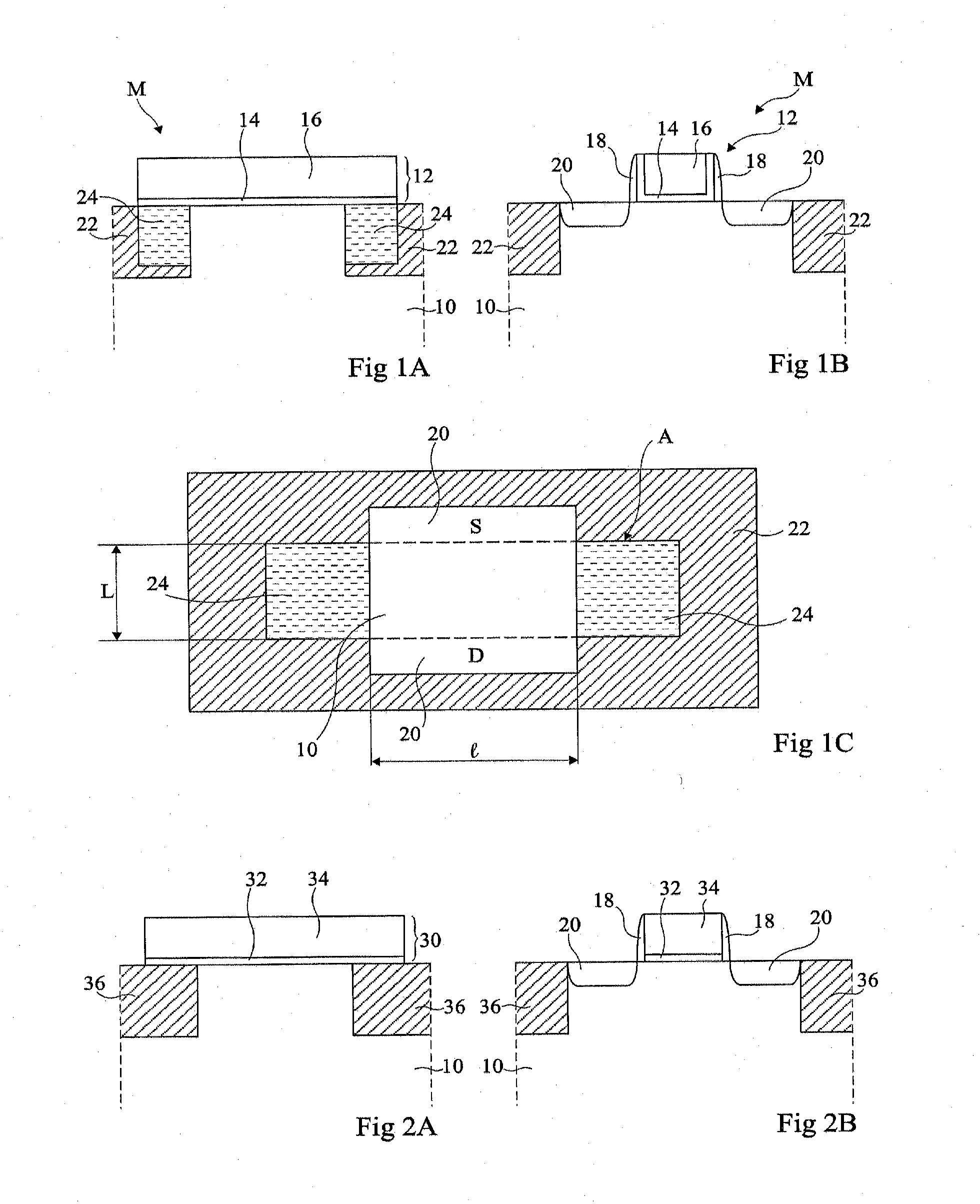
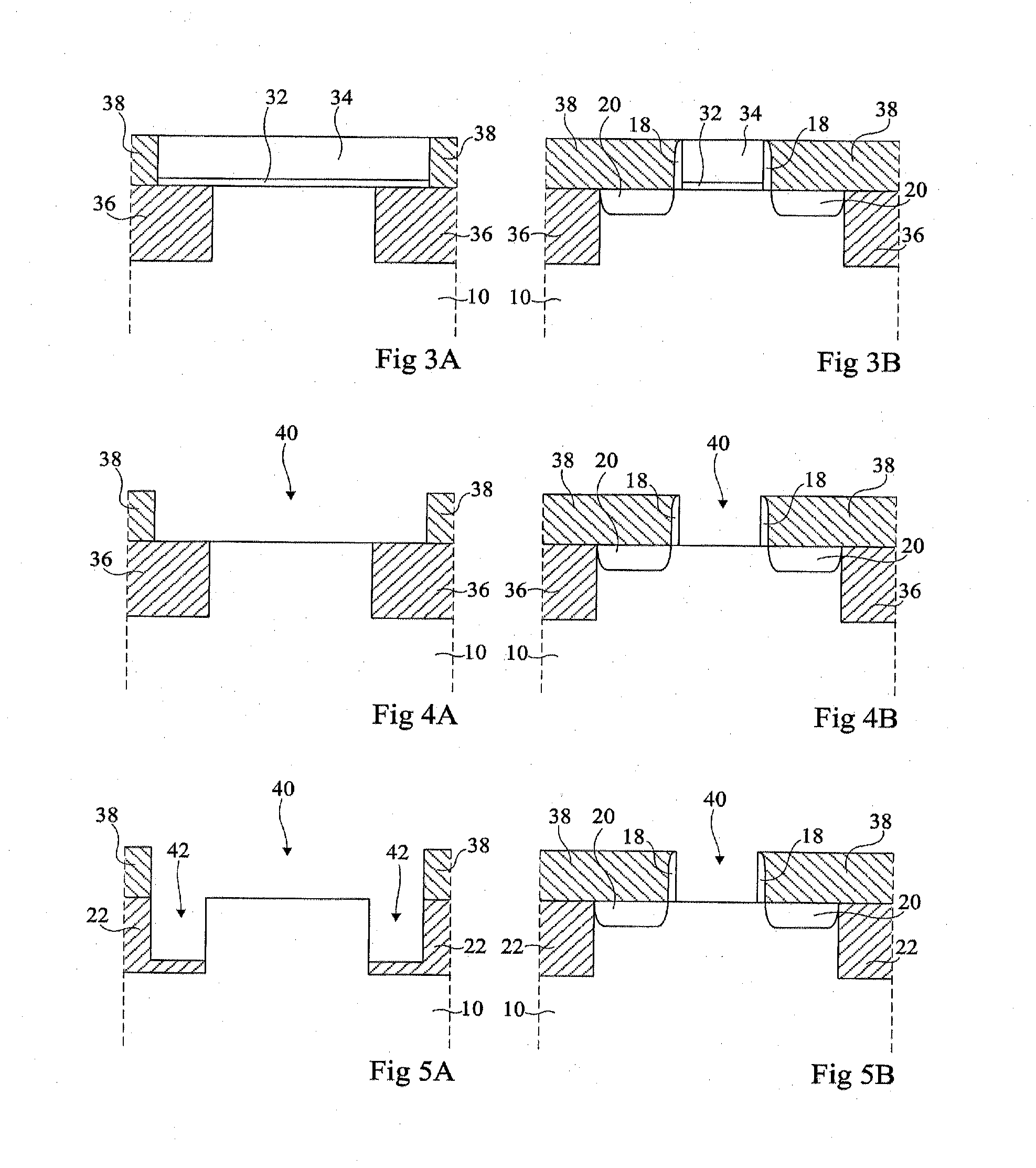
[0025]In the drawings which will be described hereafter, a single MOS transistor is shown at the surface of a substrate. It should be noted that, conventionally, many MOS transistors are formed at the surface of a same substrate, for example, in association with other electronic components.

[0026]Further, in the following description, when a material applying a strain on the adjacent semiconductor substrate will be mentioned, the considered strain may be a tensile strain or a compressive strain, according to the desired application and to the desired carrier mobility.

[0027]FIGS. 1A, 1B, and 1C illustrate, respectively in cross-section view along two perpendicular directions at the surface of a substrate and in simplified top view, a MOS transistor M obtained by a method according to an embodiment. The top view of FIG. 1C is simplified in that it does not show the insulated gate of the transistor. Conventionally, the channel distance between the source and drain regions is called the ...


PUM


Abstract

A method for manufacturing a strained channel MOS transistor including the steps of: forming, at the surface of a semiconductor substrate, a MOS transistor comprising source and drain regions and an insulated sacrificial gate which partly extends over insulation areas surrounding the transistor; forming a layer of a dielectric material having its upper surface level with the upper surface of the sacrificial gate; removing the sacrificial gate; etching at least an upper portion of the exposed insulation areas to form trenches therein; filling the trenches with a material capable of applying a strain to the substrate; and forming, in the space left free by the sacrificial gate, an insulated MOS transistor gate.

Description

CROSS REFERENCE TO RELATED APPLICATIONS[0001]This application claims the priority benefit of French patent application number 10 / 57253, filed on Sep. 13, 2010, entitled METHOD FOR MANUFACTURING A STRAINED CHANNEL MOS TRANSISTOR, which is hereby incorporated by reference to the maximum extent allowable by law.BACKGROUND OF THE INVENTION[0002]1. Field of the Invention[0003]The present invention relates to a method for manufacturing strained-channel MOS transistors.[0004]2. Discussion of the Related Art[0005]Integrated MOS transistors are formed at the surface of semiconductor substrates. They include an insulated gate formed on the surface of the substrate and source and drain regions formed in the substrate, on either side of the gate.[0006]In a semiconductor substrate, the carriers involved in N-channel or P-channel transistors do not move at the same speed. To improve the mobility of carriers, it is known to form different channel regions according to the type of carriers used. Esp...

Claims


Application Information

Patent Timeline
IPC IPC(8): H01L27/088H01L21/336
CPCH01L21/76224H01L21/76283H01L29/7846H01L29/66545H01L29/66772H01L29/165H01L29/0692
Inventor MORAND, YVESPOIROUX, THIERRYBARBE, JEAN-CHARLES
Owner STMICROELECTRONICS (GRENOBLE 2) SAS
Why Eureka
Try Eureka