Package structure
- Summary
- Abstract
- Description
- Claims
- Application Information
AI Technical Summary
Benefits of technology
Problems solved by technology
Method used
Image

Examples
first embodiment
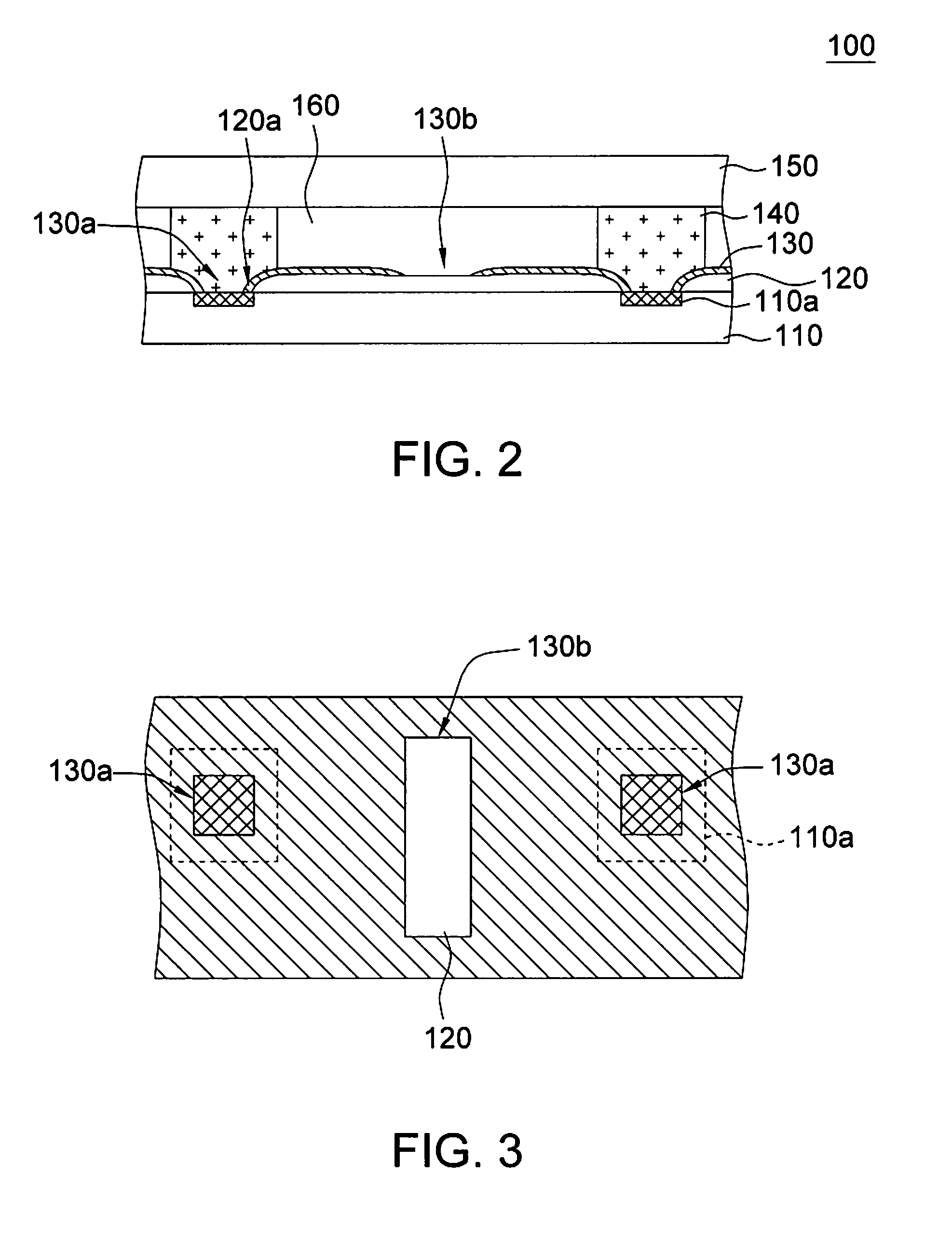
[0026]Referring to FIG. 2, a side view of a package structure according to a first embodiment of the invention is shown. The package structure 100 includes a semiconductor device 110, a first protection layer 120, a second protection layer 130 and at least one conductive bump 140. The semiconductor device 110 has at least one pad 110a. The first protection layer 120 is disposed on the semiconductor device 110 and exposes the pad 110a. The second protection layer 130 is disposed on the first protection layer 120 and has at least one first opening 130a and at least one second opening 130b. The first opening 130a exposes a partial surface of the pad 110a. The second opening 130b exposes a partial surface of the first protection layer 120. The conductive bump 140, opposite to the pad 110a, is disposed on the second protection layer 130 and coupled to the pad 110a through the first opening 130a. For the convenience of elaboration, the semiconductor device 110 has two pads 110a and two co...
second embodiment
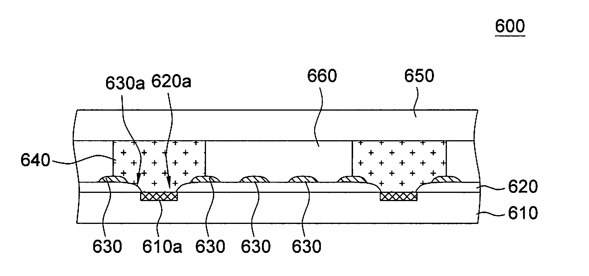
[0031]The package structure 200 of the present embodiment of the invention differs with the package structure 100 of the first embodiment mainly in the quantity of the second opening 230b of the second protection layer 230, and other similarities are not repeated here. Referring to FIG. 4, a side view of a package structure according to a second embodiment of the invention is shown. In the present embodiment of the invention, the second protection layer 230 has a plurality of first openings 230a and a plurality of second openings 230b located outside the conductive bumps 140.
[0032]On the part of the second protection layer 230, a plurality of first openings 230a expose a partial surface of the pad 110a, and a plurality of second openings 230b expose a partial surface of the first protection layer 120, wherein the sealant 160 is coupled to the first protection layer 120 through a plurality of second openings 230b to enhance the adhesion force the sealant 160 for fixing the semiconduc...
third embodiment
[0034]The package structure 300 of the present embodiment of the invention differs with the package structure 100 of the first embodiment mainly in the position of the second opening 330b of the second protection layer 330, and other similarities are not repeated here.
[0035]Referring to FIG. 6, a side view of a package structure according to a third embodiment of the invention is shown. In the present embodiment of the invention, the second protection layer 330 has a second opening 330b located under the conductive bump 340, wherein the second opening 330b exposes a partial surface of the first protection layer 120. The conductive bump 340, opposite to the pad 110a, is disposed on the second protection layer 330 and coupled to the pad 110a through the first opening 330a and coupled to the first protection layer 120 through the second opening 330b. Thus, the adhesion force between the conductive bump 340 and the semiconductor device 110 is effectively enhanced for firmly fixing the s...
PUM
 Abstract
Description
Claims
Application Information
 - R&D Engineer
- R&D Manager
- IP Professional
- Industry Leading Data Capabilities
- Powerful AI technology
- Patent DNA Extraction
Browse by: Latest US Patents, China's latest patents, Technical Efficacy Thesaurus, Application Domain, Technology Topic.
© 2024 PatSnap. All rights reserved.Legal|Privacy policy|Modern Slavery Act Transparency Statement|Sitemap