Eureka AIR delivers breakthrough ideas for toughest innovation challenges, trusted by R&D personnel around the world.

Multiple Patterning Method

a patterning method and integrated circuit technology, applied in the field of multi-pattern patterning methods of fabricating integrated circuits, can solve the problems that the accessing element, typically through a vertical plug, may not be completely compatible with the sub-lithographic dimensions

Active Publication Date: 2012-07-05
MACRONIX INT CO LTD
View PDF4 Cites 17 Cited by
  • Summary
  • Abstract
  • Description
  • Claims
  • Application Information

AI Technical Summary

Benefits of technology

[0008]The present invention is based in part on the recognition of the problems created by reducing the pitch to sub lithographic dimensions. That is, while the pitch between the lines material may be sub lithographic, the requirements for accessing the lines, typically through an access element such as a vertical plugs, may not be completely compatible with the sub lithographic dimensions. The masks used to define plugs are lithographic in size, and allowances for misalignment of masks increases the required sizes for the access areas.

Problems solved by technology

That is, while the pitch between the lines material may be sub lithographic, the requirements for accessing the lines, typically through an access element such as a vertical plugs, may not be completely compatible with the sub lithographic dimensions.

Method used


Image

  • Multiple Patterning Method
  • Multiple Patterning Method
  • Multiple Patterning Method

Examples


Embodiment Construction

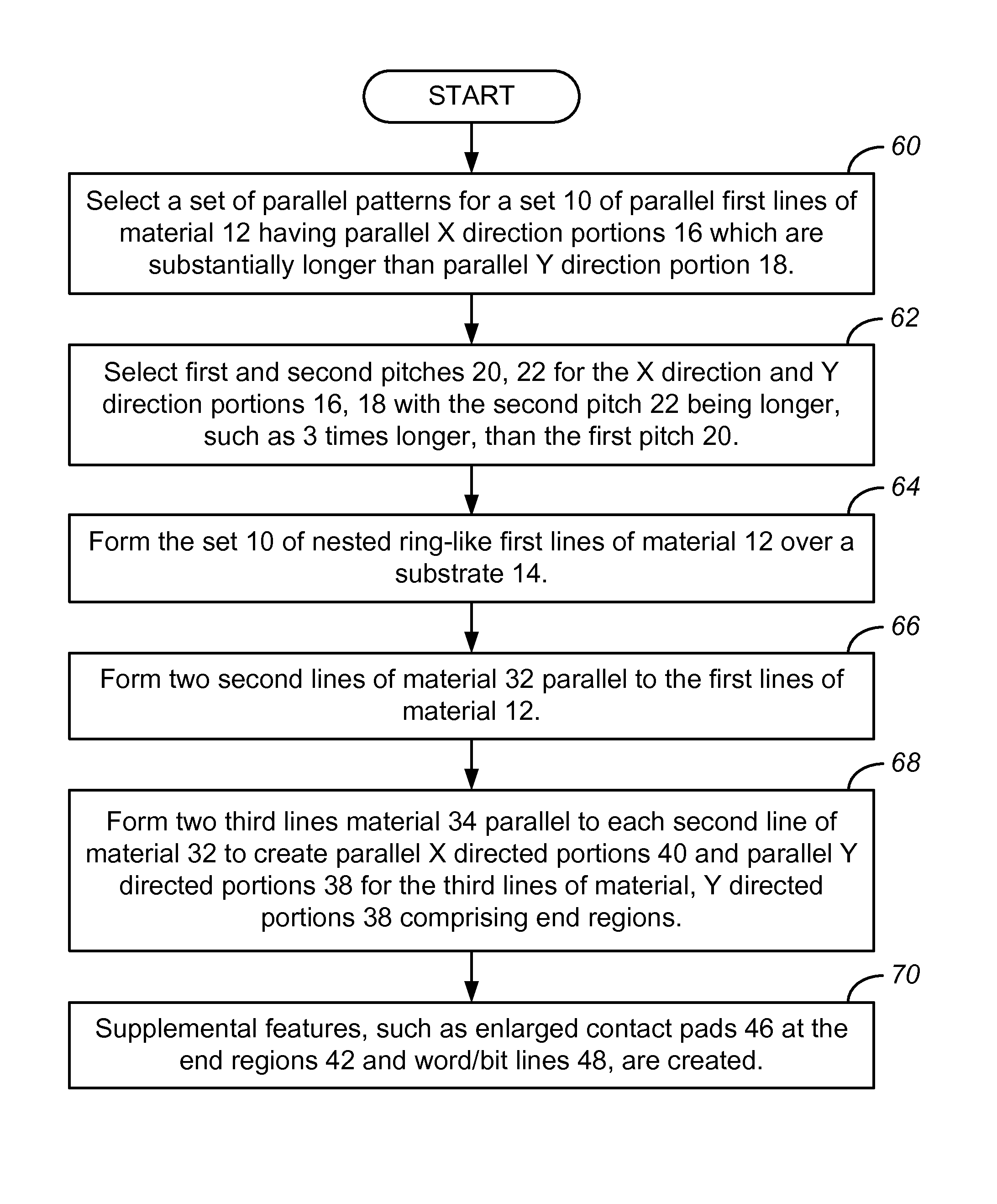
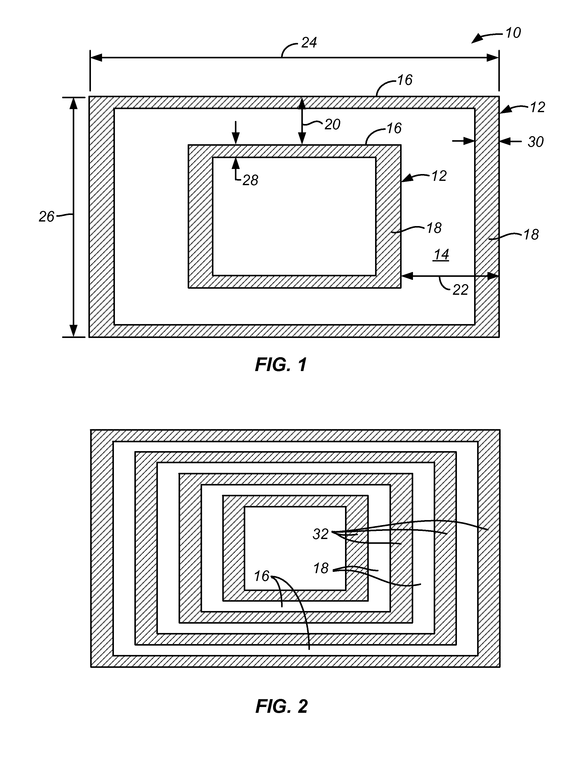
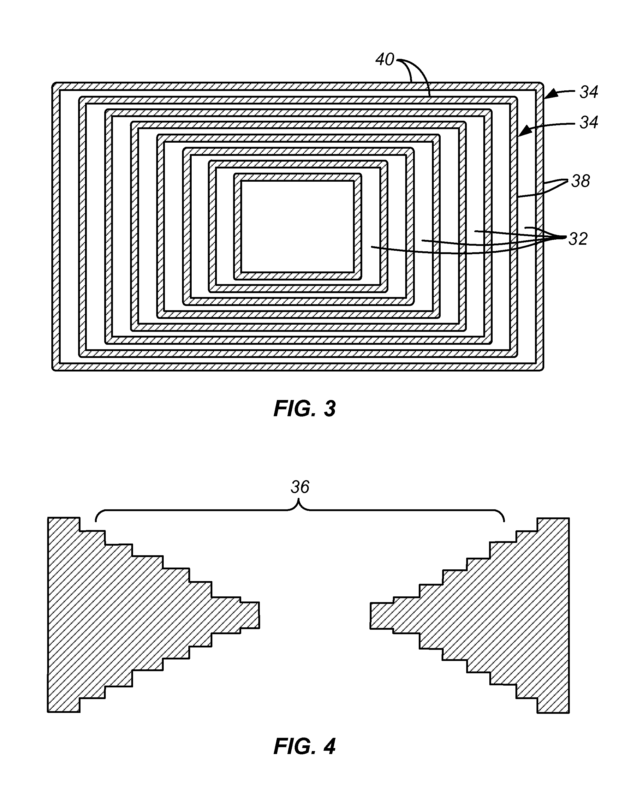
[0026]A detailed description of embodiments of the present invention is provided with reference to the FIGS. 1-33. It is to be understood and appreciated that the process steps and structures described herein do not describe a complete process flow for the manufacturing of an integrated circuit. The invention may be practiced in conjunction with various integrated circuit fabrication techniques that are conventionally used in the art, or that are hereafter developed.

[0027]The following description will typically be with reference to specific structural embodiments and methods. It is to be understood that there is no intention to limit the invention to the specifically disclosed embodiments and methods but that the invention may be practiced using other features, elements, methods and embodiments. Preferred embodiments are described to illustrate the present invention, not to limit its scope, which is defined by the claims. Those of ordinary skill in the art will recognize a variety ...


PUM


Abstract

An integrated circuit memory comprises a set of lines each line having parallel X direction line portions in a first region and Y direction line portions in a second region. The second region is offset from the first region. The lengths of the X direction line portions are substantially longer than the lengths of the Y direction line portions. The X direction and Y direction line portions have respective first and second pitches with the second pitch being at least 3 times larger than the first pitch. Contact pickup areas are at the Y direction line portions. In some examples, the lines comprise word lines or bit lines. The memory can be created using multiple patterning methods to create lines of material and then the parallel X direction line portions and parallel Y direction line portions.

Description

BACKGROUND OF THE INVENTION[0001]1. Field of the Invention[0002]The present invention relates to integration circuit fabrication, and more particularly to multiple patterning methods of fabricating integrated circuits by which access to the lines of material formed thereby is facilitated.[0003]2. Description of Related Art[0004]Integrated circuits are commonly used to make a wide variety of electronic devices, such as memory chips. There is a strong desire to reduce the size of integrated circuits, so as to increase the density of the individual components and consequently enhance the functionality of an integrated circuit. The minimum pitch on an integrated circuit (the minimum distance between the same points of two adjacent structures of the same type, e.g., two adjacent gate conductors) is often used as a representative measure of the circuit's density.[0005]Increases in circuit density often are limited by the resolution of the available photolithographic equipment. The minimum...

Claims


Application Information

Patent Timeline
IPC IPC(8): H01L29/788G03F7/20
CPCG03F7/0035H01L21/0337H01L27/11573H01L27/11565H01L27/1157H01L21/0338H10B43/35H10B43/10H10B43/40
Inventor CHEN, SHIH HUNGLUE, HANG-TING
Owner MACRONIX INT CO LTD
Why Eureka
Eureka Blog
Learn More