Imaging device with ambient light sensing means

a technology of ambient light and sensing means, which is applied in the direction of optical radiation measurement, exposure control, instruments, etc., can solve the problems of slow process and inapplicability

Active Publication Date: 2012-07-12
STMICROELECTRONICS (RES & DEV) LTD +1
View PDF9 Cites 20 Cited by
  • Summary
  • Abstract
  • Description
  • Claims
  • Application Information

AI Technical Summary

Benefits of technology

[0006]One embodiment of the present disclosure is a low-cost imaging device with a fix

Problems solved by technology

Such a process is slow and not applicable when the lens cannot be f

Method used


Image

  • Imaging device with ambient light sensing means
  • Imaging device with ambient light sensing means
  • Imaging device with ambient light sensing means

Examples


first embodiment

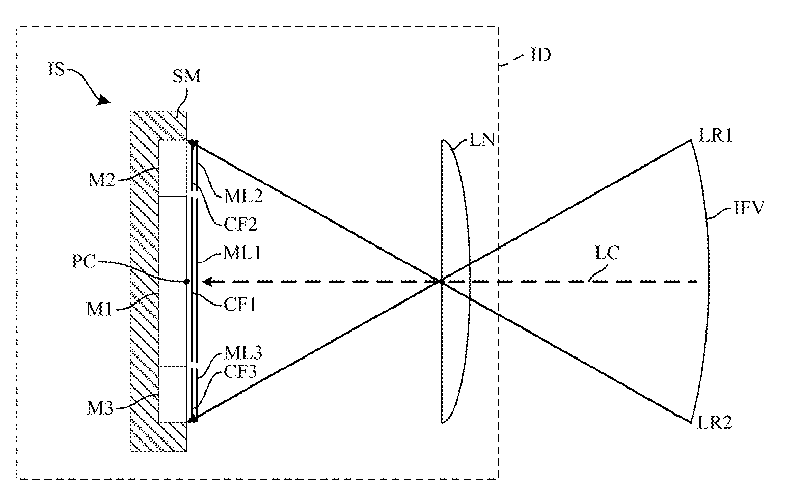
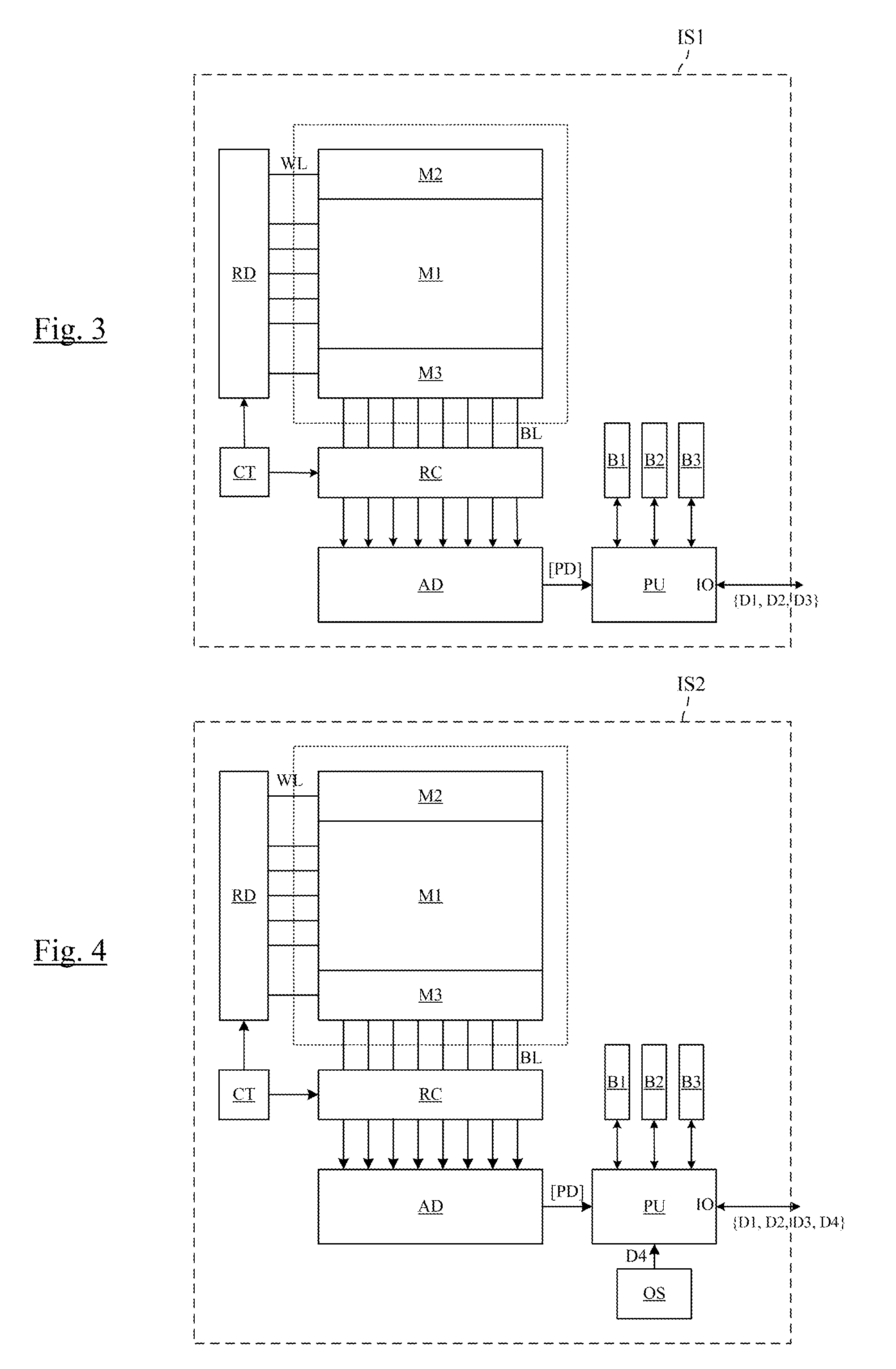
[0026]FIG. 3 schematically shows, in further detail, an image sensor IS1 according to the disclosure.

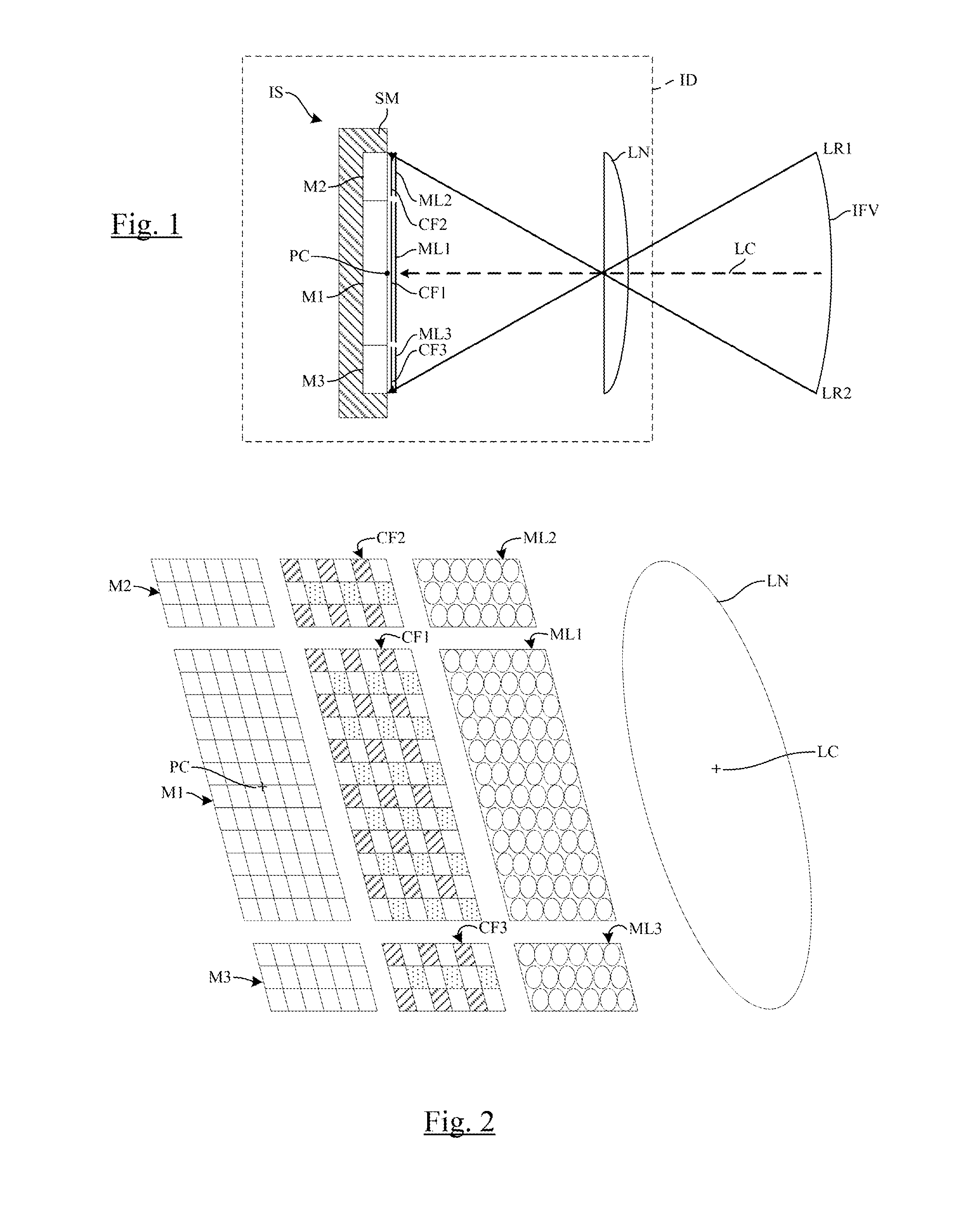
[0027]The image sensor IS1 comprises the image matrix M1, the two ambient light sensors M2, M3, a row decoder RD, a read circuit RC, a control circuit CT to control the row decoder RD and the read circuit RC, an analog to digital converter AD, a processing unit PU, three data buffers B1, B2, B3 coupled to the processing unit PU, and an input / output port IO to supply image data D1 and ambient light data or values to an external processing device. All pixels of a row are connected to the row decoder RD via a word line WL, and all pixels of a column are connected to the read circuit RC via a bit line BL.

[0028]The capture of an image and ambient light sensing is performed row by row, and comprises an exposition phase and a read phase. The image sensor IS is exposed to incident light rays, which are focused onto individual pixels. Photons of the light rays cause electron-hole pairs to be ...

second embodiment

[0034]FIG. 4 schematically shows an image sensor IS2 according to the disclosure. The image sensor IS2 comprises, in addition to the elements described above in relation with FIG. 3, an orientation sensor OS. The orientation sensor OS supplies a orientation data D4 to the processing unit PU. The orientation sensor may be a MEMS (Micro-Electro Mechanical) sensor.

[0035]In this embodiment, the processing unit PU uses orientation data D4 to process the data D2, D3 received from the ambient light sensors M2, M3. For example, if the device is rotated 180°, the ambient light sensor M3 is activated while ambient light sensor M2 is de-activated. If the device is rotated 90° or 270°, the data D2, D3 from sensors M2, M3 may be averaged. Data D4 may also be supplied to the exterior via the port IO.

[0036]The following data processing methods may be implemented by the processing unit PU to process the ambient light data D2, D3 supplied by the ambient light sensors M2, M3:

Fk(Li)=AVG(D2,D3)  {metho...


PUM


Abstract

An imaging device includes a fixed focused lens, an image sensor having a image matrix of a plurality of pixels arranged on a semiconductor substrate and supplying image data, and electronic means for reading the image matrix. The image sensor also comprises at least two ambient light sensors arranged on the semiconductor substrate on opposite sides of the image matrix, and configured to capture an ambient light intensity through the fixed lens, and the electronic means is also configured to read the two ambient light sensors and to supply ambient light data and the image data.

Description

BACKGROUND[0001]1. Technical Field[0002]The present disclosure relates to an imaging device comprising a fixed focused lens and an image sensor comprising a plurality of pixels arranged on a semiconductor substrate and supplying image data and electronic means for reading the image matrix.[0003]2. Description of the Related Art[0004]Imaging devices typically comprise a lens and an image sensor in the form of a semiconductor chip comprising a matrix of pixels. These devices may be used for a wide range of applications including “machine vision” such as visual inspection of merchandise or facial recognition wherein an image is captured and processed. The device may further include an ambient light sensor (“ALS”) functionality, for example to process a captured image depending on the amount of ambient light present, or to adjust a display intensity on a television monitor. Currently, such devices are being integrated into many devices including mobile telephones, personal digital assis...

Claims


Application Information

Patent Timeline
IPC IPC(8): H04N5/235
CPCG01J1/4204G03B7/0997H04N5/2351H04N23/71
Inventor CELLIER, ALEXANDREDESCHAMPS, BENOITRAYNOR, JEFF
Owner STMICROELECTRONICS (RES & DEV) LTD
Why Eureka
Try Eureka