Resistance weld additive manufacturing

a technology of additive manufacturing and resistive welds, which is applied in the direction of manufacturing tools, manufacturing apparatus, transportation and packaging, etc., can solve the problems of reducing the properties of many alloys, affecting the performance of the alloy, and affecting the quality of the alloy,

Inactive Publication Date: 2012-07-19
SIEMENS ENERGY INC
View PDF25 Cites 17 Cited by
  • Summary
  • Abstract
  • Description
  • Claims
  • Application Information

AI Technical Summary

Problems solved by technology

The above-described processes have disadvantages and limitations.
For example, some of the processes are exceedingly slow and cost prohibitive if many parts are required.
Further, except for parts where sintered powder deposits result in adequate material properties, deposition of metal by these processes usually requires complete remelting and solidification.
Such remelting degrades the properties of many alloys.
The properties and geometry of the underlying substrate are also negatively affected by the heat of subsequent layered processing.
Also, certain alloys are available only as a thin sheet because they require specific environmental heat treatment to optimize properties, and as such, providing the alloy in powder form as required for the above processes is not possible.
Ultrasonic consolidation avoids the melting of the deposited material and many of the drawbacks of the above processes, but it has its own limitations.
For example, available power limits the process to soft alloys (e.g. aluminum).
Available tool forces and available tool rigidity limit accuracy of fabrication.
Tools are of limited durability; in particular sonotrode wear is high.
Material is often transferred to the sonotrode, causing maintenance issues and yield losses.
Finally, a thickness of deposited material is limited to a “ribbon” typically of 0.15 mm (0.006″) thickness, and therefore the process is slow and often involves incremental machining steps.

Method used


Image

  • Resistance weld additive manufacturing
  • Resistance weld additive manufacturing
  • Resistance weld additive manufacturing

Examples


Embodiment Construction

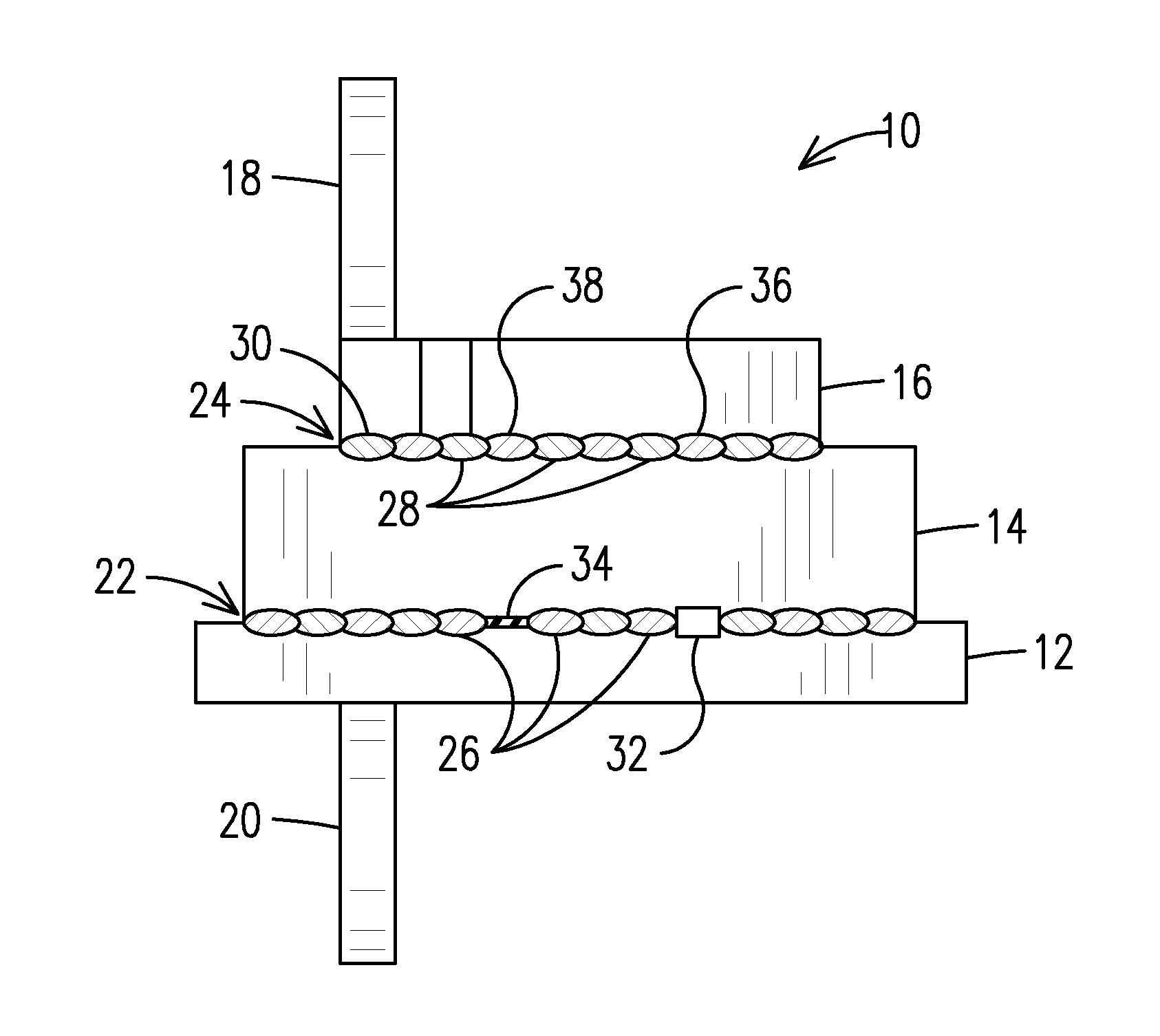
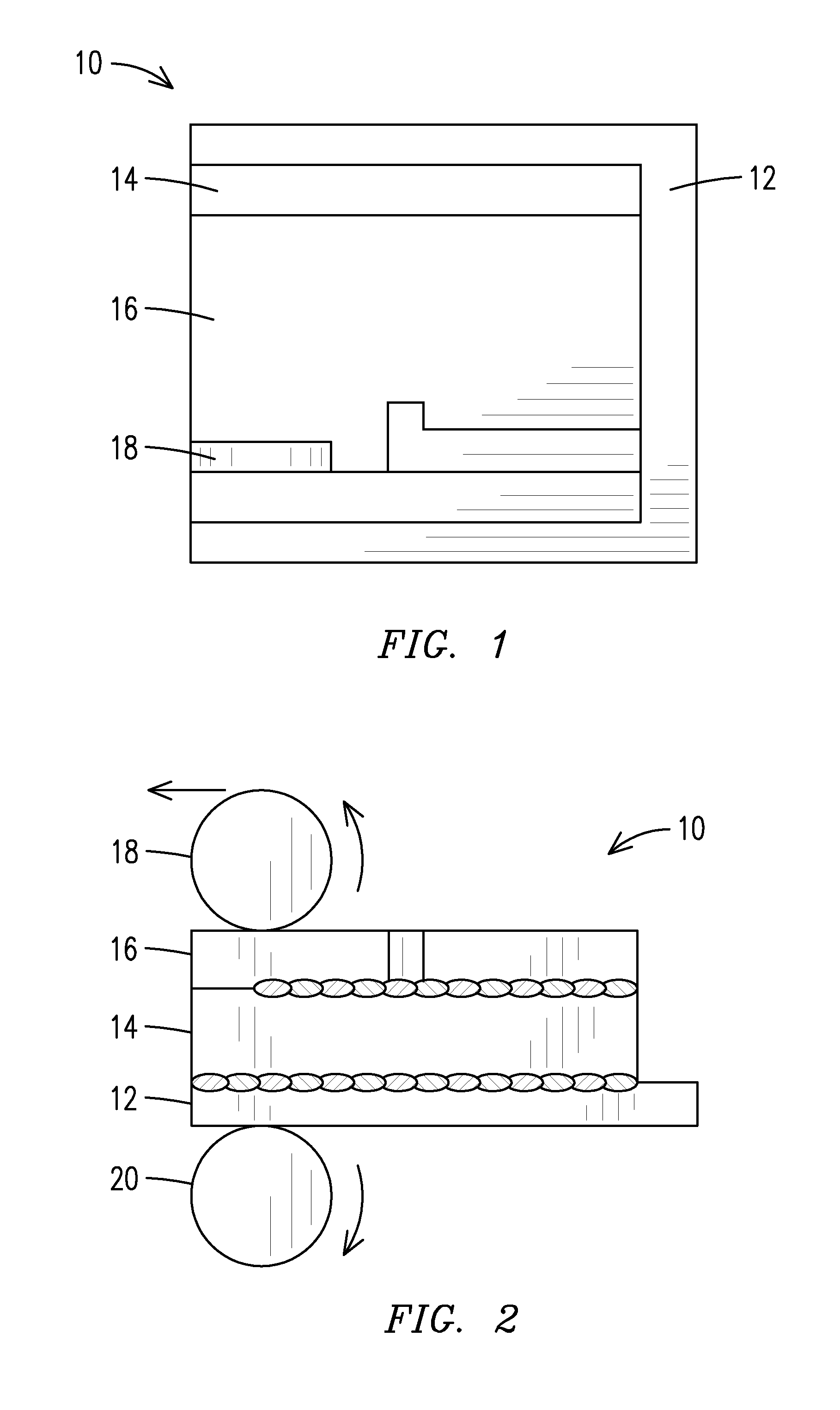
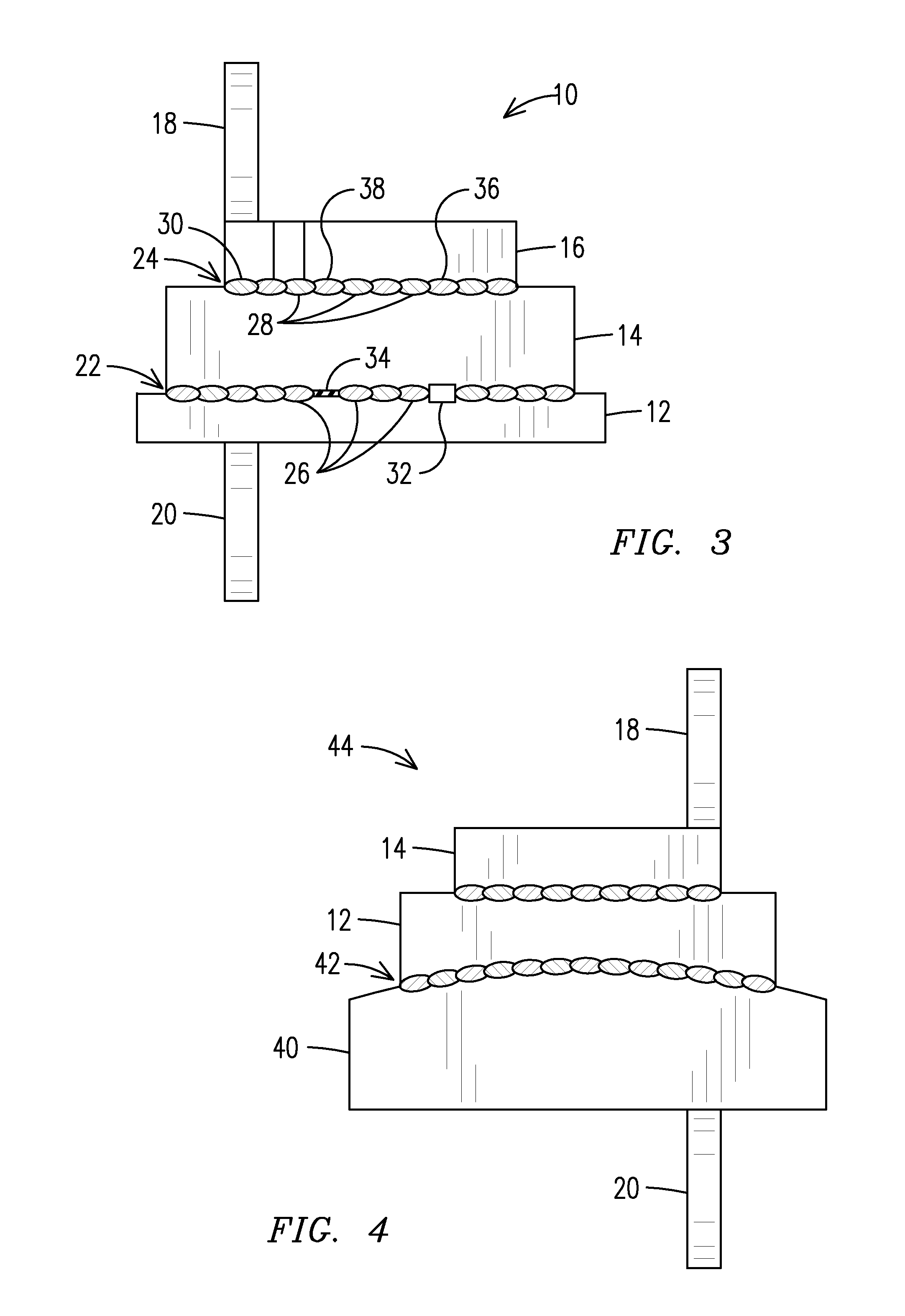
[0012]The present inventor has devised an innovative, yet simple, additive manufacturing process that is not subject to many of the limitations of conventional additive manufacturing techniques. The process uses resistance welding to join multiple layers of a substrate where each layer of the substrate forms a portion of an assembled structure. The assembled structure may be the final structure, or may be subject to subsequent machining to become a final structure.

[0013]Individual layers may be fabricated using conventional cutting processes, (e.g. milling, sawing, water jet, plasma, electro spark discharge etc) prior to being assembled, but any fabricating technique is acceptable. Each pre-assembled layer may be fabricated to a layer final shape such that no subsequent machining will be required, or it may be fabricated to a layer assembly shape in anticipation of subsequent machining of the assembled structure to reach a final structure.

[0014]Resistance welding involves straddling...


PUM

PropertyMeasurementUnit
thicknessaaaaaaaaaa
resistanceaaaaaaaaaa
areaaaaaaaaaaa

Abstract

A method of additive manufacturing, including resistance welding together contacting surfaces of adjacent substrate sheets, wherein weld nuggets overlap adjacent weld nuggets and collectively form a respective layer that bonds a portion of an entirety of an area of the respective contacting surfaces, thereby forming an assembled structure of at least three substrate sheets, wherein each substrate sheet includes a respective portion of a final structure.

Description

FIELD OF THE INVENTION[0001]The invention relates to a method of additive manufacturing. Specifically, the invention relates to resistance welding multiple layers of substrate material together to form an assembled structure.BACKGROUND OF THE INVENTION[0002]Additive manufacturing is generally considered the buildup of three dimensional objects by multiple layer processing, each layer representing a portion of the three dimensional object. Multiple additive manufacturing processes are in use, including stereo lithography. In stereo lithography light, (i.e. often a laser beam) is programmed to traverse a liquid that cures and becomes solid when exposed to the laser wavelength, each pass of the laser representing one layer. Certain photopolymers are most often used for this.[0003]The three dimensional object may also be produced directly by energy sources of high enough power to melt a metal or alloy used in the three dimensional object. For example, high power laser beams are commonly...

Claims


Application Information

Patent Timeline
Patent Type & Authority Applications(United States)
IPC IPC(8): B32B15/00B23K11/00
CPCB23K11/061C22C19/07B23K35/38Y10T428/12493B23K35/0261Y10T428/12451B23K35/0233B32B15/00
Inventor BRUCK, GERALD J.
Owner SIEMENS ENERGY INC
Why Eureka
Try Eureka