Gate signal line drive circuit and display device

a technology of gate signal and drive circuit, which is applied in the direction of electric digital data processing, instruments, computing, etc., can solve the problems of increasing the circuit size of the shift register basic circuit, and achieve the effect of improving the voltage quality of the gate signal outpu

Active Publication Date: 2012-07-26
JAPAN DISPLAY INC
View PDF1 Cites 6 Cited by
  • Summary
  • Abstract
  • Description
  • Claims
  • Application Information

AI Technical Summary

Benefits of technology

[0009]The invention has been made in view of such a problem, and it is an object of the invention to provide a gate signal line driving circuit capable of improving the vol

Problems solved by technology

This increases the circuit size of

Method used


Image

  • Gate signal line drive circuit and display device
  • Gate signal line drive circuit and display device
  • Gate signal line drive circuit and display device

Examples


first embodiment

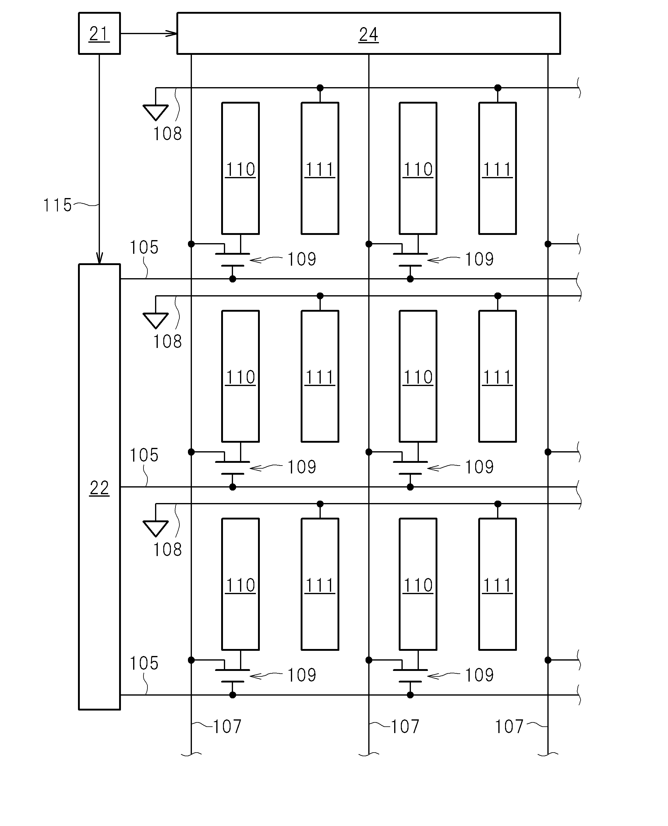
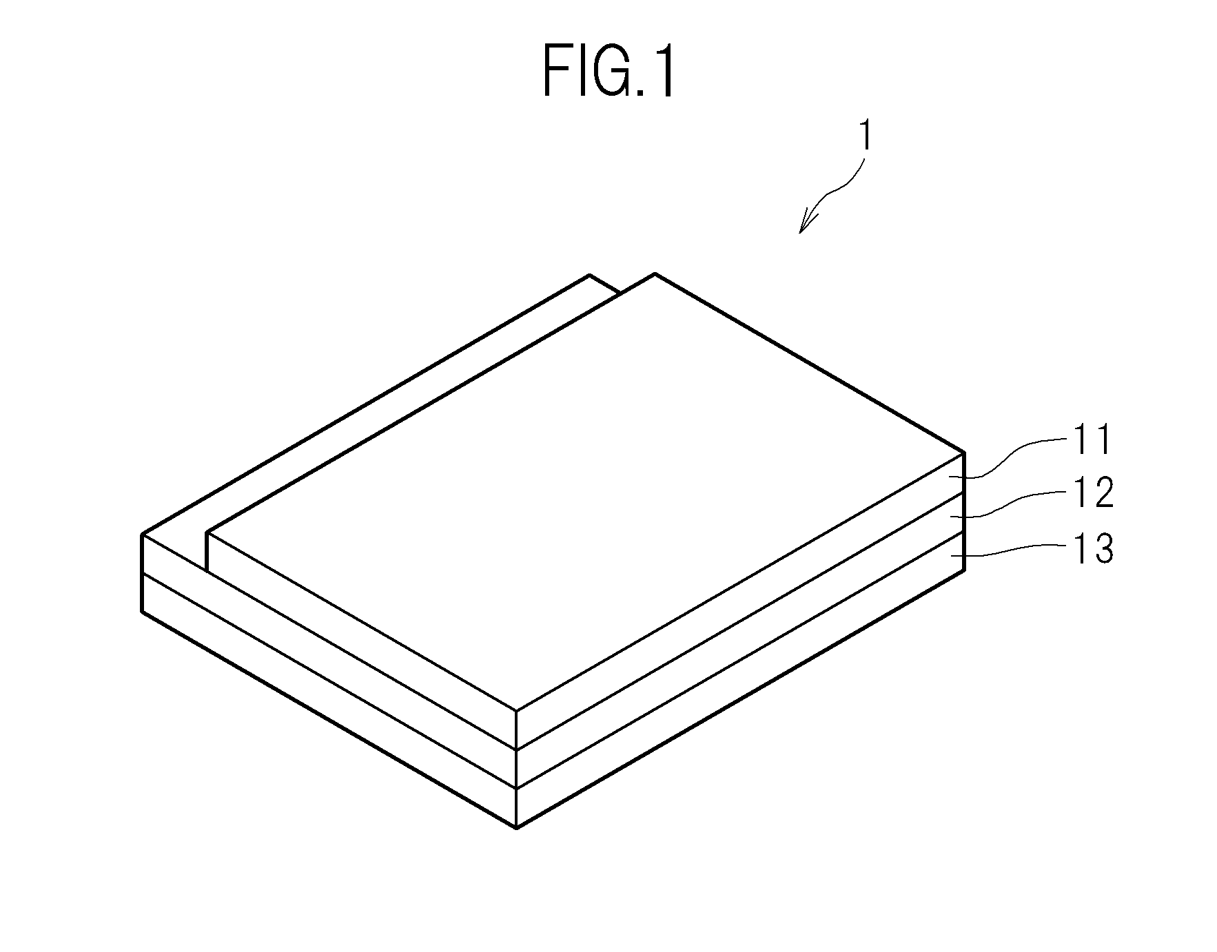
[0041]A display device according to a first embodiment of the invention is an IPS (In-Plane Switching) liquid crystal display device 1, for example. As shown in an overall perspective view of the liquid crystal display device 1 according to the present embodiment shown in FIG. 1, the liquid crystal display device 1 is configured to include a TFT substrate 12, a filter substrate 11 which faces the TFT substrate 12 and in which a color filter is provided, a liquid crystal material sealed in a region interposed between both the substrates, and a backlight 13 disposed adjacent to a surface of the TFT substrate 12 not facing the filter substrate 11. Here, a gate signal line 105, a video signal line 107, a pixel electrode 110, a common electrode 111, a TFT 109, and the like, which will be described later, are disposed on the TFT substrate (refer to FIG. 3).

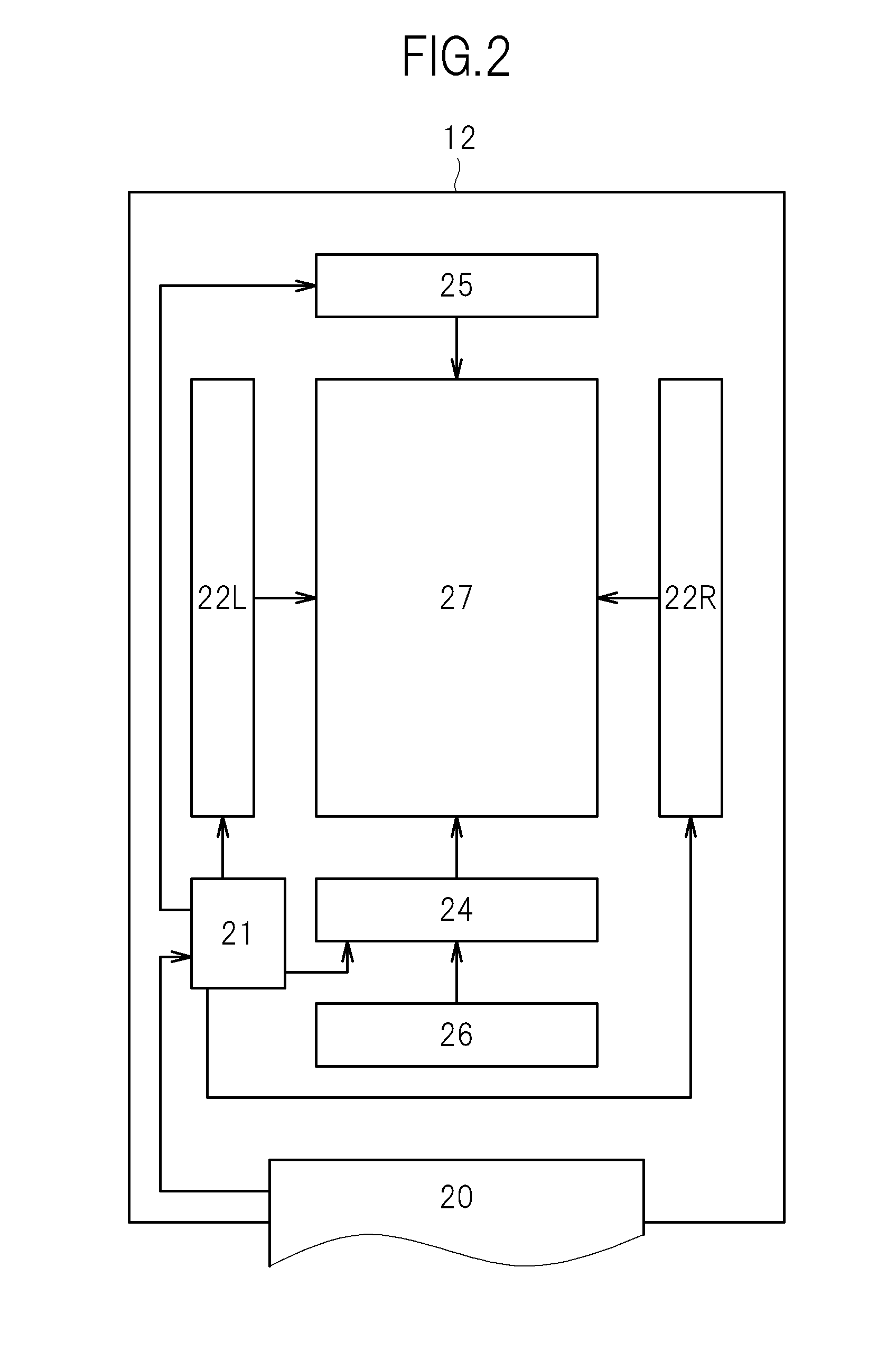
[0042]FIG. 2 is a block diagram showing the configuration of the TFT substrate 12 of the liquid crystal display device 1 according to ...

second embodiment

[0102]A display device according to a second embodiment of the invention has basically the same configuration as the display device according to the first embodiment. The main difference between the display device according to the second embodiment and the display device according to the first embodiment is that the gate signal line driving circuit 22 according to the present embodiment can perform bidirectional driving so that either forward driving or reverse driving can be selectively performed.

[0103]In the gate signal line driving circuit 22 according to the first embodiment, both the gate signal line driving circuit 22R shown at the right side of FIG. 2 and the gate signal line driving circuit 22L shown at the left of FIG. 2 perform forward driving. In contrast, in the gate signal line driving circuit 22 according to the present embodiment, the gate signal line driving circuit 22L shown at the left of FIG. 2 is not driven when the gate signal line driving circuit 22R shown at t...

third embodiment

[0120]A display device according to a third embodiment of the invention has basically the same configuration as the display device according to the second embodiment. Similar to the gate signal line driving circuit 22 according to the second embodiment, a gate signal line driving circuit 22 according to the present embodiment can perform bidirectional driving so that either forward driving or reverse driving can be selectively performed. In addition, the main difference between the display device according to the third embodiment and the display device according to the second embodiment is the configuration of the shift register basic circuit SR.

[0121]FIG. 9 is a circuit diagram of an n-th shift register basic circuit SRn of a gate signal line driving circuit 22R according to the present embodiment which performs forward driving. Compared with the circuit diagram of the n-th shift register basic circuit SRn according to the second embodiment shown in FIG. 7, the n-th shift register ...


PUM


Abstract

A gate signal line driving circuit includes plural basic circuits, each outputting to a gate signal line a gate signal which is high during a high signal period and low during a low signal period. Each of the basic circuits includes: agate line high voltage application circuit which is turned on in accordance with the high signal period to apply the high voltage to the gate signal line; a gate line low voltage application circuit which is turned on in accordance with the low signal period to apply the low voltage to the gate signal line; and a second gate line low voltage application circuit which is turned on to apply the low voltage to the gate signal line in at least a part of a period between turning off the gate line high voltage application circuit and turning on the gate line low voltage application circuit.

Description

CROSS-REFERENCE TO RELATED APPLICATION[0001]The present application claims priority from Japanese application JP 2011-013512 filed on Jan. 25, 2011, the content of which is hereby incorporated by reference into this application.BACKGROUND OF THE INVENTION[0002]1. Field of the Invention[0003]The present invention relates to a gate signal line driving circuit and a display device using the same.[0004]2. Description of the Related Art[0005]In known display devices, such as liquid crystal display devices, a method is often adopted in which agate signal line driving circuit including plural shift register basic circuits, which output to plural gate signal lines gate signals that have a high voltage in order, is formed on the same substrate as a thin film transistor (hereinafter, referred to as a TFT) disposed in a display unit, example. A gate signal line driving circuit in the related art is disclosed in JP 2010-113247A.[0006]For example, in a shift register basic circuit disclosed in J...

Claims


Application Information

Patent Timeline
IPC IPC(8): G09G5/00
CPCG09G3/006G09G3/3677G09G3/3688G09G2310/0297G09G2310/0251G09G2310/0281G09G2310/0283G09G2310/0248G09G3/3611G09G2310/0286G09G2310/0289G09G2310/08
Inventor ABE, HIROYUKIMAKI, MASAHIROSATO, HIDEOKOMATSU, HIROAKI
Owner JAPAN DISPLAY INC
Why Eureka
Try Eureka