Semiconductor memory apparatus

a memory device and semiconductor technology, applied in the direction of information storage, static storage, digital storage, etc., can solve the problems of increasing the offset voltage the inability of the bit line sense amplifier circuit to correctly amplify data, etc., and achieve the effect of reducing the power noise of the bit line sense amplifier circui

Inactive Publication Date: 2012-07-26
SK HYNIX INC
View PDF4 Cites 10 Cited by
  • Summary
  • Abstract
  • Description
  • Claims
  • Application Information

AI Technical Summary

Benefits of technology

[0008]A semiconductor memory apparatus capable of reducing power noise of a bit line sense amplifier circuit is described herein.

Problems solved by technology

However, if the offset voltage is greater than a difference in voltage between the main bit line and the sub bit line, the bit line sense amplifier circuit cannot correctly amplify data.
Particularly, when the bit line sense amplifier circuit uses an over driving voltage so as to reduce an amplification time thereof, the offset voltage of the bit line sense amplifier circuit is increased more due to power noise.

Method used


Image

  • Semiconductor memory apparatus
  • Semiconductor memory apparatus
  • Semiconductor memory apparatus

Examples


Embodiment Construction

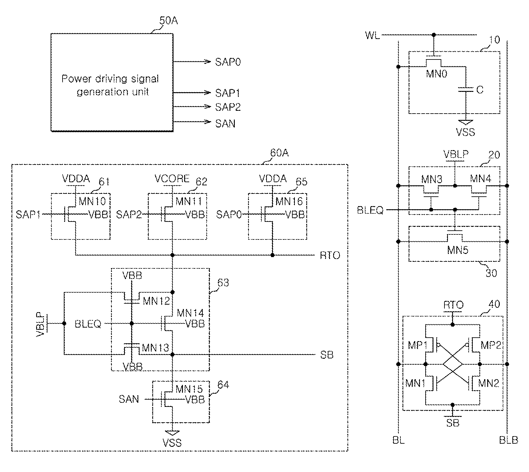
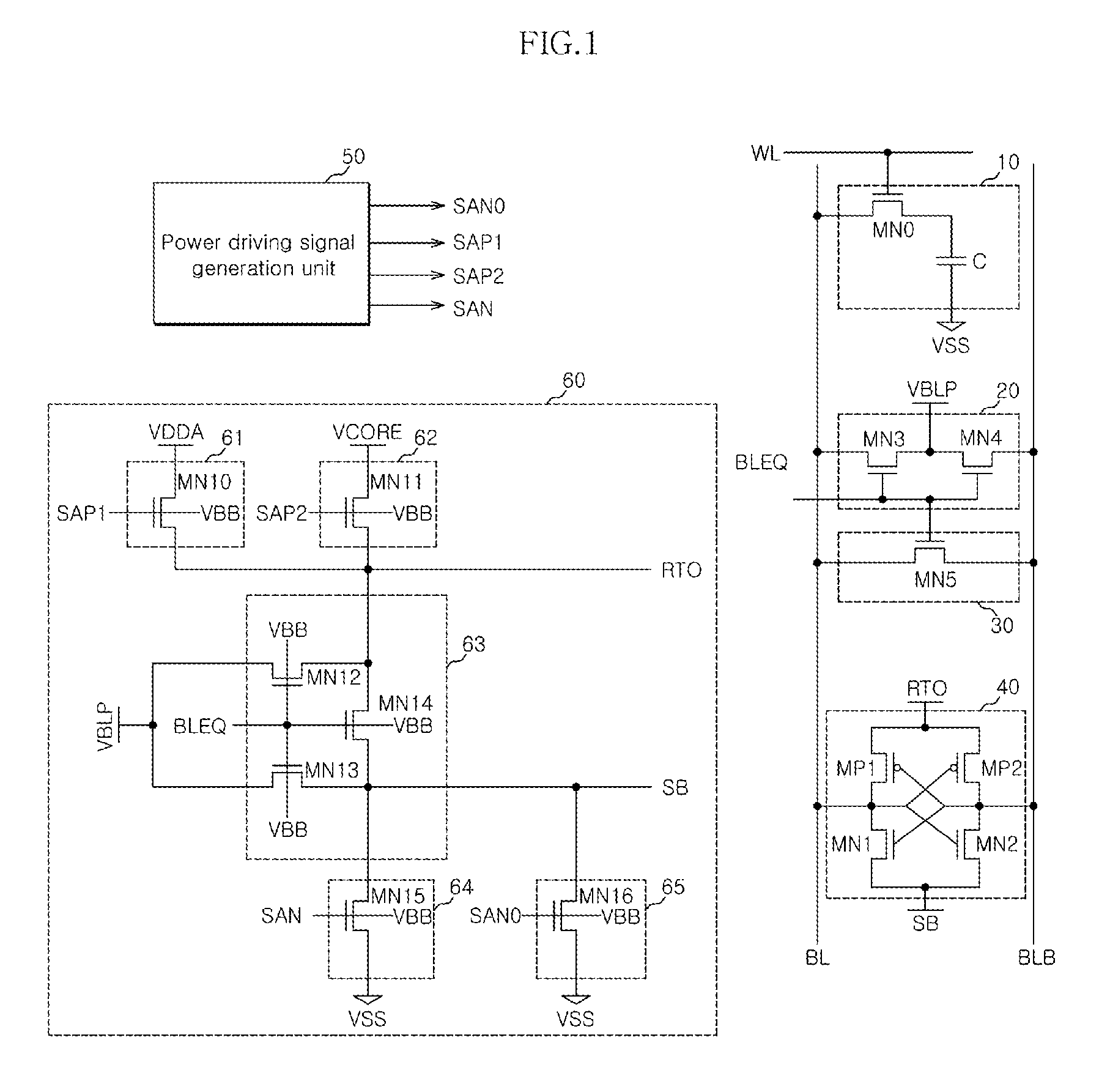
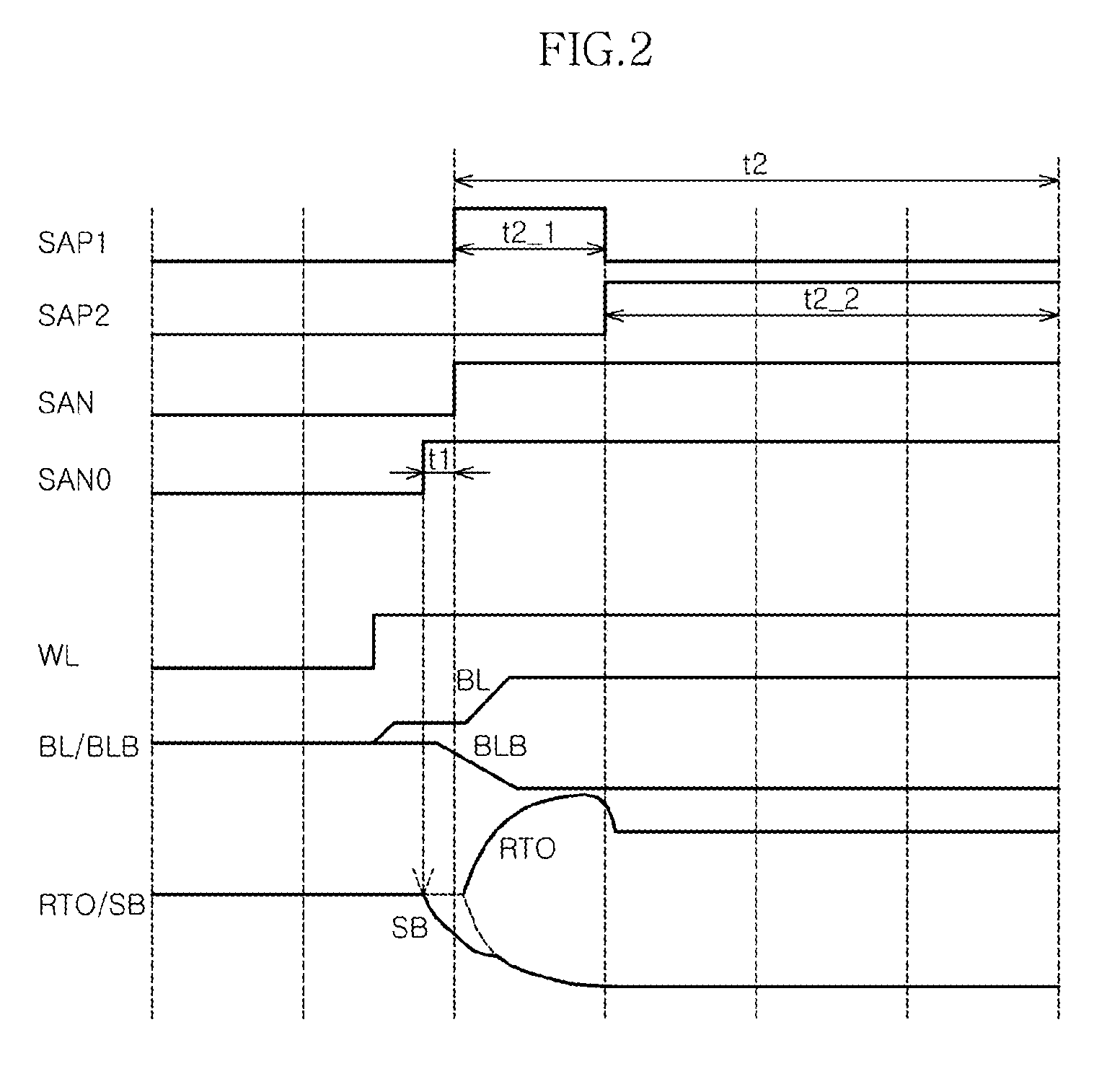
[0022]Hereinafter, a semiconductor memory apparatus according to embodiments of the present invention will be described below with reference to the accompanying drawings through example embodiments.

[0023]For reference, a term, symbol or sign used when designating an element or block in the drawings and detailed description may be represented for each specific unit as occasion demands, and therefore, a like term, symbol or sign cannot designate a like element or block in the entire circuit. Further, data stored in the semiconductor memory apparatus is divided into a high level (H) or low level (L) corresponding to a voltage level thereof, and may be represented by ‘1’ or ‘0,’ respectively. Here, values of the data are divided depending on the level of voltage and the amplitude of current. In the case of binary data, the high level is defined as a high voltage, and the low level is defined as a voltage lower than the high level.

[0024]FIG. 1 is a configuration diagram of a semiconducto...


PUM


Abstract

A semiconductor memory apparatus includes a bit line sense amplifier unit and a driving voltage supply unit. The bit line sense amplifier unit senses and amplifies a signal provided from a memory cell using a pull-up driving voltage provided through a pull-up power line and a pull-down driving voltage provided through a pull-down power line. The driving voltage supply unit supplies the pull-down driving voltage having a first pull-down driving force during a first amplification period, and supplies the pull-down driving voltage having a second pull-down driving force greater than the first pull-down driving force during a second amplification period after the first amplification period.

Description

CROSS-REFERENCES TO RELATED APPLICATION[0001]The present application claims priority under 35 U.S.C. §119(a) to Korean application number 10-2011-0007291, filed on Jan. 25, 2011, in the Korean Intellectual Property Office, which is incorporated herein by reference in its entirety as set forth in full.BACKGROUND[0002]1. Technical Field[0003]The present invention relates to a semiconductor memory apparatus, and more particularly, to a technology for sensing and amplifying data of a memory cell using a bit line sense amplifier circuit.[0004]2. Related Art[0005]In general, a semiconductor memory apparatus receives external power so as to generate an internal voltage having various voltage levels, and operates an internal circuit using the internal voltage. As the semiconductor memory apparatus is more highly integrated, the voltage levels of the external power and the internal voltage are gradually lowered. Particularly, a bit line sense amplifier circuit for sensing and amplifying data...

Claims


Application Information

Patent Timeline
Patent Type & Authority Applications(United States)
IPC IPC(8): G11C7/12G11C7/06
CPCG11C11/4094G11C11/4091G11C5/14G11C7/06G11C7/12
Inventor LEE, KANG SEOLYUN, TAE SIK
Owner SK HYNIX INC
Why Eureka
Try Eureka