Printed circuit board

Inactive Publication Date: 2008-01-03
HON HAI PRECISION IND CO LTD
View PDF7 Cites 2 Cited by
  • Summary
  • Abstract
  • Description
  • Claims
  • Application Information

AI Technical Summary

Benefits of technology

[0005]An exemplary printed circuit board (PCB) includes at least one power trace. A plurality of etched portions are defined in the at least one power trace, acting as electromagnetic bandgaps for transferring resonant frequencies produced around the at least one power trace to avoid working frequencies of the PCB, thereby reducing power noise around the at least one power trace.

Problems solved by technology

Generally speaking, noise can not be avoided in PCBs, such as coupling / crosstalk between signals, electro-magnetic interference (EMI) from high-frequency signals, and power noise from power delivery systems, especially the simultaneous switching noise (SSN) whose resonant frequencies may interfere with working frequencies of the PCBs.
However, this method uses precious space for arranging the de-coupling capacitors, and also increases design complexity of the PCB.

Method used


Image

  • Printed circuit board
  • Printed circuit board
  • Printed circuit board

Examples


Embodiment Construction

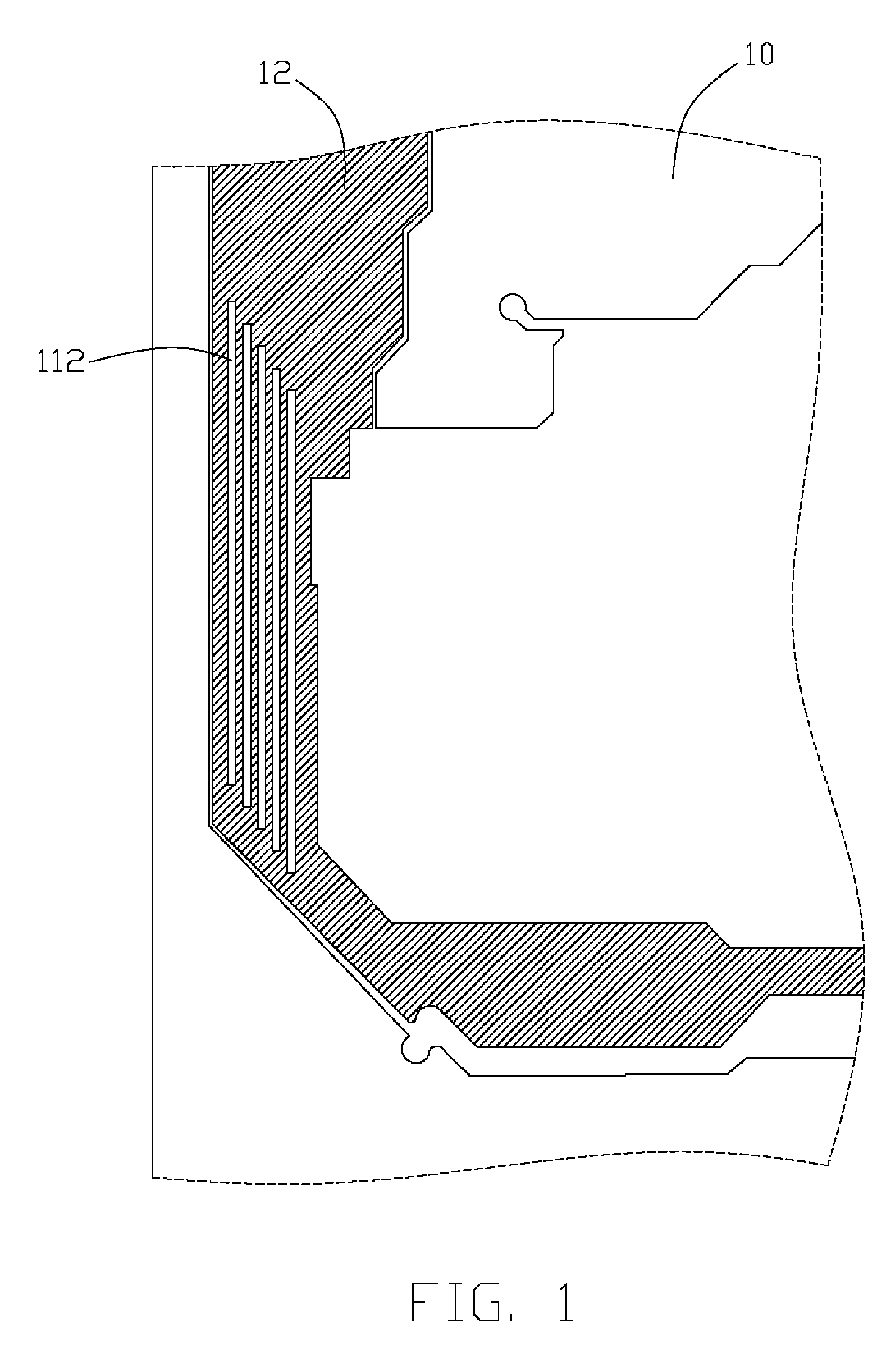
[0010]Referring to FIG. 1, a printed circuit board (PCB) 10 in accordance with a first preferred embodiment of the present invention is shown. The PCB 10 includes a power delivery system having at least one power trace 12 arranged therein, and other traces are not shown. The power delivery system can be in a signal layer or a power layer of the PCB 10. A plurality of parallel lengthwise (along the power trace 12) etched grooves 112 are defined in the power trace 12 and act as electromagnetic bandgaps. The grooves 112 will increase partial inductance of the power trace 12, and resonant frequencies produced around the power trace 12 will be transferred, thus the transferred resonant frequencies can avoid working frequencies of the PCB, thereby reducing power noise around the power trace 12. Other power traces or power planes can also be designed like the power trace 12 for reducing the power noise therein.

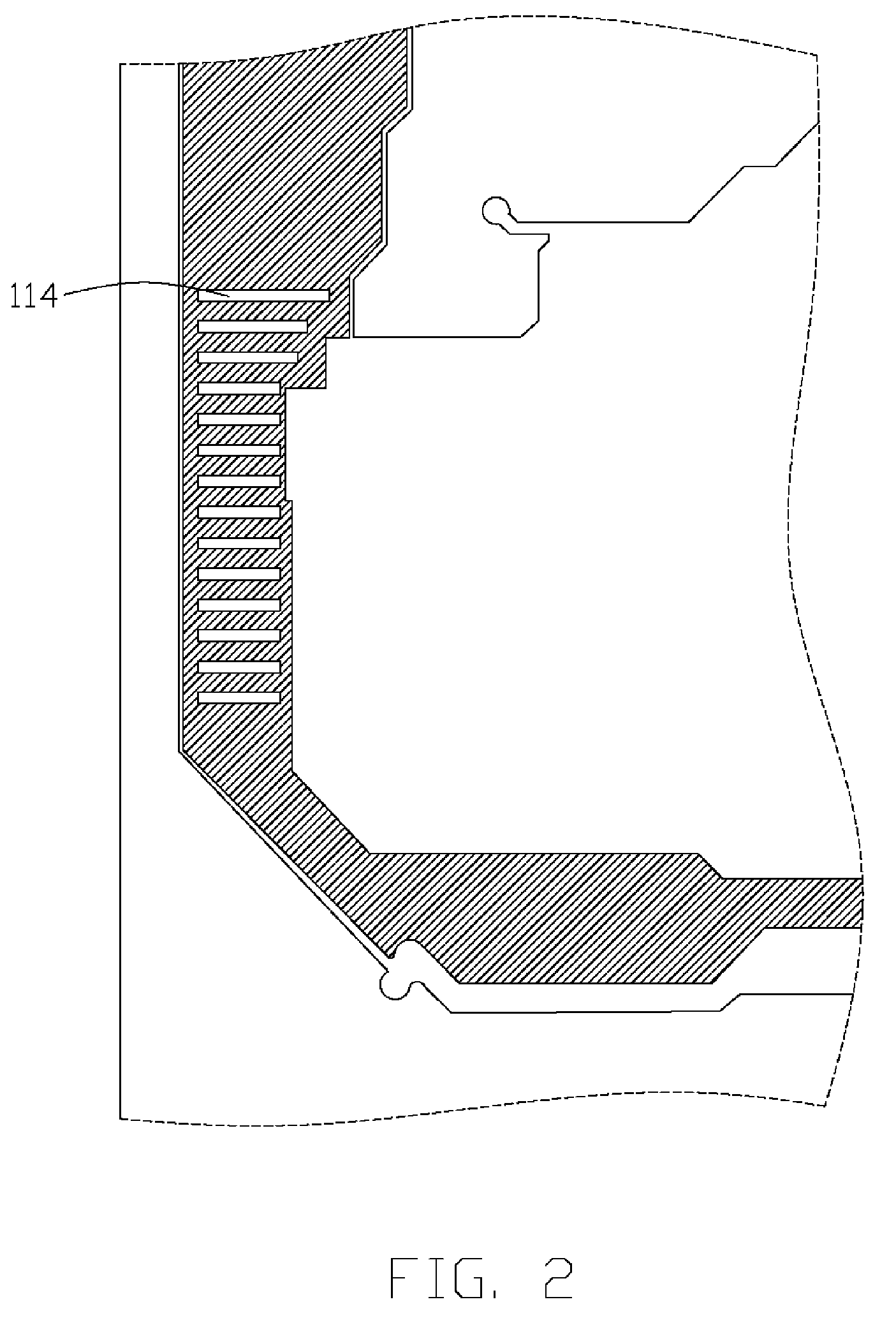
[0011]Referring also to FIG. 2, a printed circuit board (PCB) in accordance with...


PUM


Abstract

A printed circuit board (PCB) includes at least one power trace. A plurality of etched portions are defined in the at least one power trace, acting as electromagnetic bandgaps for transferring resonant frequencies produced around the at least one power trace to avoid working frequencies of the PCB, thereby reducing power noise around the at least one power trace.

Description

1. FIELD OF THE INVENTION[0001]The present invention relates to printed circuit boards (PCBs), and more particularly, to a PCB for reducing power noise therein.2. DESCRIPTION OF RELATED ART[0002]Generally speaking, noise can not be avoided in PCBs, such as coupling / crosstalk between signals, electro-magnetic interference (EMI) from high-frequency signals, and power noise from power delivery systems, especially the simultaneous switching noise (SSN) whose resonant frequencies may interfere with working frequencies of the PCBs.[0003]Some methods are applied for reducing power noise from power delivery systems, and a conventional method is to add some de-coupling capacitors in a PCB. The de-coupling capacitors can store redundant energy therein, and release the energy to the power delivery system at an appropriate moment. However, this method uses precious space for arranging the de-coupling capacitors, and also increases design complexity of the PCB.[0004]What is desired, therefore, i...

Claims


Application Information

Patent Timeline
IPC IPC(8): H01R12/00
CPCH05K1/0216H05K1/0265H05K2201/0979H05K2201/0969H05K2201/09336
Inventor LAI, YING-TSOPAI, YU-CHANGHSU, SHOU-KUO
Owner HON HAI PRECISION IND CO LTD
Why Eureka
Try Eureka